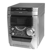
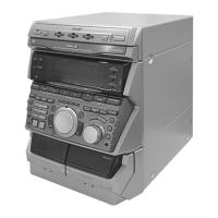
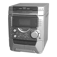
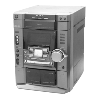
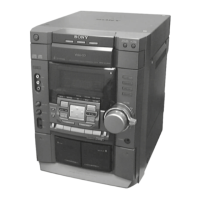
HCD-VX77/VX77J
48
48
Function
41 TE I Tracking error signal input
42 CE I Center servo analog input
43 RFDC I RF signal input
44 ADI0 O Test pin (Not used)
45 AVSS0 — Analog ground
46 IGEN I Power supply pin operational amplifiers
47 AVDD — Analog power supply
48 ASYO O EFM full swing output
49 ASYI I Asymmetry comparate voltage input
50 RFAC I EFM signal input
51 AVSS1 — Analog ground
52 CLTV I Control voltage input for master VCO
53 FILO O Filter output for master PLL
54 FILI I Filter input for master PLL
55 PCO O Charge-pump output for master PLL
56 AVDD1 — Analog power supply
57 BIAS I Asymmetry circuit constant current input
58 VCTL I Control voltage input for variable pitch PLL
59 V16M I/O 16.9344MHz output (Not used)
60 VPCO O Charge-pump output for variable pitch PLL (Not used)
61 DVDD2 — Digital power supply
62 ASYE I Asymmetry circuit ON/OFF (Connected to +5V.)
63 MD2 I Digital-out ON/OFF control (Connected to +5V.)
64 DOUT O Digital-out output
65 LRCK O 48-bit slot D/A interface, LR clock output
66 PCMD O 48-bit slot D/A interface, Serial deta output
67 BCLK O 48-bit slot D/A interface, bit clock output
68 EMPH O Playback disc output in emphasis mode (Not used)
69 XTSL I X’tal selection input pin
70 DVSS2 — Digital ground
71 XTAI I X’tal oscillator circuit input
72 XTAO O X’tal oscillator circuit output (Not used)
73 SOUT O
74 SOCK O (Not used)
75 XOCT O
76 SQSO O Sub-Q serial output
77 SQCK I Clock input for SQSO read-out
78 SCSY I Sub-code input
79 SBSO O Sub-P through Sub-W serial output (Not used)
80 EXCR I Clock input for SBSO read-out
Pin No.
1 DVDD0 — Digital power supply
2 XRST I System reset
3 MUTE I Muting selection pin
4 DATA I Serial data input, supplied from CPU
5 XLAT I Latch input, supplied from CPU
6 CLOK I Serial data transfer clock input, supplied from CPU
7 SENS O SENS output
8 SCLK I SENS serial data read-out clock
9 ATSK I/O Input pin for anti-shock (Ground)
10 WFCK O WFCK (Write Frame Clock) output (Not used)
11 XUGF O XUGF output (Not used)
12 XPCK O XPCK output (Not used)
13 GFS O GFS output (Not used)
14 C2P0 O C2PO output
15 SCOR O Sub-code sync output
16 CM4 O 4.2336MHz output (Not used)
17 WDCK O 48-bit slot D/A interface word clock (Not used)
18 DVSS — Digital ground
19 COUT O Numbers of track counted signal output (Not used)
20 MIRR O Mirror signal output (Not used)
21 DFCT O Defect signal output (Not used)
22 FOK O Focus OK output (Not used)
23 PWM1 I (Not used)
24 LOCK I/O GFS in sampled by 460Hz (Not used)
25 MDP O Output to control spindle motor servo
26 SSTP I Input signal to detect disc inner most trak
27 FST0 O 2/3 divider output (Not used)
28 DVDD1 — Digital power supply
29 SFDR O
30 SRDR O
31 TFDR O
32 TRDR O
33 FFDR O
34 FRDR O
35 DVSS1 — Digital ground
36 TEST I
37 TES1 I
38 VC I Center voltage input
39 FE I FOCUS error signal input
40 SE I Sled error signal input
Pin Name
Pin No.
I/O
7-23. IC PIN FUNCTIONS
• IC101 DIGITAL SIGNAL PROCESSOR (CXD3008Q) (BD Board)
Sled drive output
Tracking drive output
Focus drive output
TEST pin connected normally ground
Pin Name I/O Function