RDR-HX680/HX780/HX785/HX980/HX1080
4-44-3
4-2. SCHEMATIC DIAGRAMS
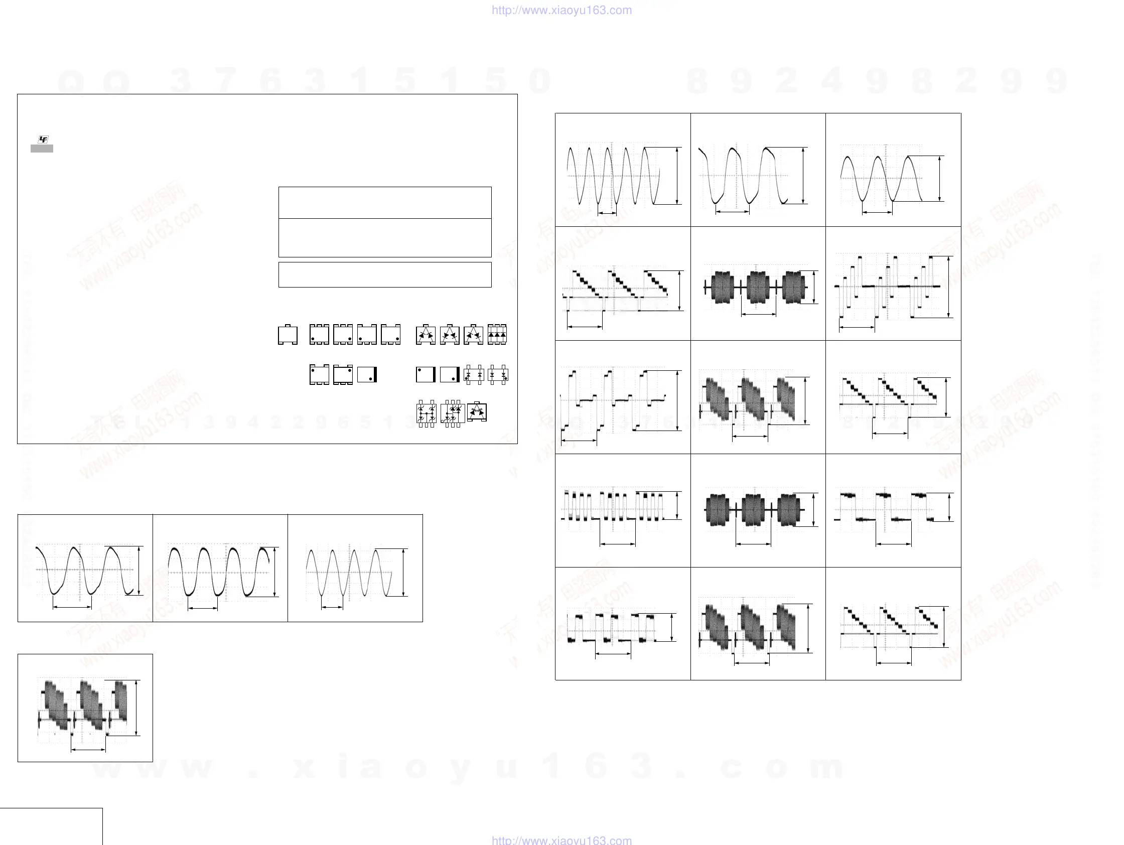
WAVEFORMS
AV-133/134 BOARD
5.0 Vp-p
30.5 ns
66.6 ns
5.0 Vp-p
1 IC101 qd (X101)
H
1.4 Vp-p
5 JA401 4
1.2 Vp-p
H
q; JA501 7 B OUT
2 IC101 q; (X102)
1.2 Vp-p
H
qd JA501 qg R OUT
1.7 Vp-p
9 JA402 Y OUT
H
6 JA402 Pb OUT
1.0 Vp-p
H
qf JA501 ql V OUT
2.2Vp-p
H
4.0 Vp-p
54.2 ns
1.4 Vp-p
H
qa JA501 qg C OUT
3 IC601 6 (X601)
7 JA402 Pr OUT
1.0 Vp-p
H
1.2 Vp-p
H
qs JA501 qa G OUT
1.8 Vp-p
H
4 JA401 3
8 JA402 V OUT
2.1 Vp-p
H
qg JA501 ql Y OUT
1.8Vp-p
H
WAVEFORMS
AV-133/134 FR-291
RD-066
(For printed wiring boards)
• : Uses unleaded solder.
• : Pattern from the side which enables seeing.
(The other layers’ patterns are not indicated)
• Through hole is omitted.
• There are a few cases that the part printed on diagram
isn’t mounted in this model.
• C : panel designation
(For schematic diagrams)
• All capacitors are in µF unless otherwise noted. pF : µµF.
50V or less are not indicated except for electrolytics and
tantalums.
• All resistors are in ohms, 1/4 W (Chip resistors : 1 /10 W) un-less
otherwise specified.
kΩ=1000Ω, MΩ=1000kΩ.
• Caution when replacing chip parts.
New parts must be attached after removal of chip.
Be careful not to heat the minus side of tantalum capacitor, be-
cause it is damaged by the heat.
• All variable and adjustable resistors have characteristic curve B,
unless otherwise noted.
• 2 : non flammable resistor
• 5 : fusible resistor
• C : panel designation
• f : internal component
• C : adjustment for repair
• G : IN/OUT direction of (+/–) B line
• U : B+ Line
• V : B– Line
• Circled numbers refer to waveforms.
•Voltages are dc between measurement point and ground.
THIS NOTE IS COMMON FOR SCHEMATIC DIAGRAMS
(In addition to this, the necessary note is printed in each block)
• Chip parts.
Transistor Diode
21
3
12
3
21
3
21
3
345
21
123
654
EB
C
31
5
5
2
46
123
54
43
12
5
4
1 3
12
43
312
45
534
12
34
21
12
43
46
2
5
31
12
4
3
64
1
3
Note : The components identified by mark 0 or dotted
line with mark 0 are critical for safety.
Replace only with part number specified.
Note : Les composants identifiés par une marque 0 sont
critiques pour la sécurité.
Ne les remplacer que par une pièce portant le numéro
spécifié.
FR-291 BOARD
H
1.0 Vp-p
1 J201 VIDEO IN
7
RD-066 BOARD
3.2 Vp-p
40.7 ns
59 ns
3.7 Vp-p
1 IC1001 (AF1) 2 IC5103 wd (X5101)
2.1 Vp-p
40 ns
3 IC5602 wd (X5502)
• Readings are taken with a color-bar signals on DVD reference
disc.
• Readings are taken with a digital multimeter (DC 10MΩ).
•Voltage variations may be noted due to normal production tol-
erances.
When indicating parts by reference number, please
include the board name.
w
w
w
.
x
i
a
o
y
u
1
6
3
.
c
o
m
Q
Q
3
7
6
3
1
5
1
5
0
9
9
2
8
9
4
2
9
8
T
E
L
1
3
9
4
2
2
9
6
5
1
3
9
9
2
8
9
4
2
9
8
0
5
1
5
1
3
6
7
3
Q
Q
TEL 13942296513 QQ 376315150 892498299
TEL 13942296513 QQ 376315150 892498299
http://www.xiaoyu163.com
http://www.xiaoyu163.com



 To Next Page