Do you have a question about the Sony STR-DG710 and is the answer not in the manual?
| RMS rated power | 600 W |
|---|---|
| Audio output channels | 5.1 channels |
| Supported radio bands | AM, FM |
| Radio Data System (RDS) | Yes |
| I/O ports | AV in/out Video in/out HDMI in/out D-Sub DM |
| Connectivity technology | Wired |
| Headphone outputs | 1 |
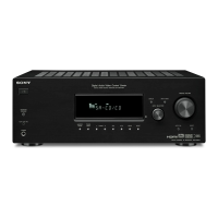
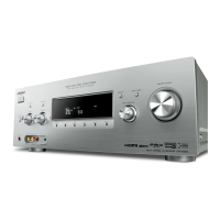
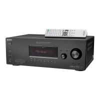
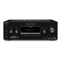
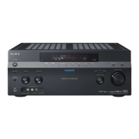
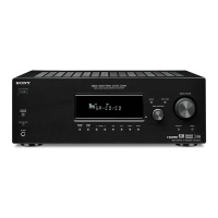
| Product color | Black |
| Dimensions (WxDxH) | 430 x 157.5 x 310 mm |
| Weight | 7800 g |
|---|
Details output power for US/Canadian models.
Details output power for AEP/UK/AUS models.
Details output power for SP/MY/TH models.
Frequency response range for analog inputs.
Details analog input/output parameters.
S/N ratio for digital inputs.
FM tuning range, antenna type, and frequency.
AM tuning scale, antenna, and frequency.
Specifications for video and component connections.
Power needs and consumption figures by area code.
Unit dimensions and weight.
List of included accessories with the receiver.
Procedure for checking AC leakage on US models.
Note on replacing damaged ICs on the HDMI RE board.
Part numbers corresponding to model identification.
Notes on reusing and handling chip components.
Guidelines and characteristics of unleaded solder.
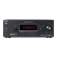
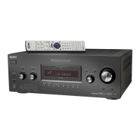
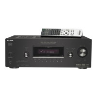
Introduction to basic receiver operations and setup.
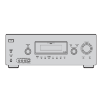
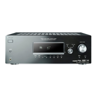
Identification and function of front panel controls.
Indicators for sound modes and input signals.
XM Radio and system status indicators.
Indicators showing active playback channels.
Connectors for digital audio/video and component video.
Ports for analog audio, speakers, and antennas.
Operation of power, input selection, and volume controls.
Controls for tuning, menu navigation, and display.
Step-by-step guide to removing the unit's case.
Procedure for accessing the back panel components.
Guide to removing the front panel assembly.
Procedures for DIGITAL, MAIN, and STANDBY boards.
AM channel step selection and display segment testing.
Key check, swap all, and shipment modes.
DCAC factory test and software version display modes.
Procedure to clear preset sound fields for reset.
Checking data lines for DCAC DSP integrity.
Testing DCAC board using test tone output.
Procedure for testing FM reception sensitivity with a signal generator.
Visual map showing the location of all internal circuit boards.
Block diagram illustrating tuner and audio signal flow.
Block diagram of the digital signal processing path.
Block diagram showing video signal paths and switching.
Block diagram of the HDMI interface circuitry.
Block diagram for the XM Satellite Radio module signal flow.
Block diagram of button inputs and display signal logic.
Block diagram of audio output stages and power supply.
Waveforms from IC1301 on the Digital Board.
Waveforms from XM and HDMI RE Board ICs.
Component placement on the Main Board, Side A.
Component placement on the Main Board, Side B.
First part of the Main Board schematic diagram.
Second part of the Main Board schematic diagram.
Component placement on the Digital Board, Side A.
Component placement on the Digital Board, Side B.
First schematic part for the Digital Board.
Second schematic part for the Digital Board.
Third schematic part for the Digital Board.
Component layout and schematic for the DCAC Board.
Component layout and schematic for the Power Key Board.
Component placement on the Video 3 Board.
Component placement on the Video Board.
Schematic diagrams for Video 3 and Video Boards.
Component placement on the HDMI RE Board, Side A.
Component placement on the HDMI RE Board, Side B.
First schematic part for the HDMI RE Board.
Second schematic part for the HDMI RE Board.
Component placement on the XM Board, Side A.
Component placement on the XM Board, Side B.
Schematic diagram for the XM Board.
Component placement on the Display Board.
Schematic diagram for the Display Board.
Component placement on the Standby Board.
Schematic diagram for the Standby Board.
Component placement on the DCDC Board.
Schematic diagram for the DCDC Board.
Block diagrams for key ICs on the Main Board.
Block diagrams for initial Digital Board ICs.
Block diagrams for additional Digital Board ICs.
Block diagrams for IC1401 and IC1452 on Digital Board.
Block diagrams for ICs on the Video Board.
Block diagrams for IC3503 and IC3507 on HDMI RE Board.
Block diagrams for other HDMI RE Board ICs.
Block diagrams for HDMI RE and XM Board ICs.
Block diagrams for XM and Display Board ICs.
Block diagrams for ICs on the DCDC Board.
Pin descriptions for IC1501 from pin 1 to 56.
Pin descriptions for IC1501 from pin 57 to 120.
Pin descriptions for IC1907 from pin 1 to 48.
Pin descriptions for IC1907 from pin 49 to 99.
Pin descriptions for IC1907 from pin 100 to 120.
Pin descriptions for IC3511 from pin 1 to 70.
Pin descriptions for IC3511 from pin 71 to 128.
Pin descriptions for IC3513 from pin 1 to 60.
Pin descriptions for IC3513 from pin 61 to 80.
Exploded view of the unit's case and related parts.
Exploded view of the front panel assembly.
Exploded view of the back panel assembly and connectors.
Exploded view of the chassis and major internal components.
List of parts for the DCAC Board.
List of parts for the DCDC Board.
List of capacitors for the DCDC Board.
List of capacitors for the Digital Board (Part 1).
List of capacitors for the Digital Board (Part 2).
List of connectors, diodes, and ferrite beads.
List of resistors and transistors by reference number.
List of resistors R1153 through R1711 on the Main Board.
List of resistors R1712 through R1964 on the Main Board.
List of network resistors and vibrator components.
List of resistors R106 through R110.
List of capacitors for the HDMI RE Board.
List of ICs and transistors for the HDMI RE Board.
List of connectors and diodes for the HDMI RE Board.
List of resistors R3570-R3799 for HDMI RE Board.
List of components for the Headphone Board.
List of capacitors C400 through C801 for the Main Board.
List of capacitors C802 through C832 for the Main Board.
List of connectors, diodes, and ICs for the Main Board.
List of transistors and resistors for the Main Board.
List of resistors R537 through R748 on the Main Board.
List of miscellaneous parts for the Main Board.
List of relays, terminals, and power key components.
List of rotary encoders and tactile switches.
List of capacitors for the Standby Board.
List of capacitors for the Video Board.
List of resistors for the Video Board.
List of capacitors and connectors for the XM Board.
List of ICs, transistors, and resistors for the XM Board.
List of miscellaneous parts for the XM Board.
List of standard remote commanders and antennas.
List of instruction manuals and conversion adapters.
Initial release of the manual.
Update including Thai model information.