– 107 –
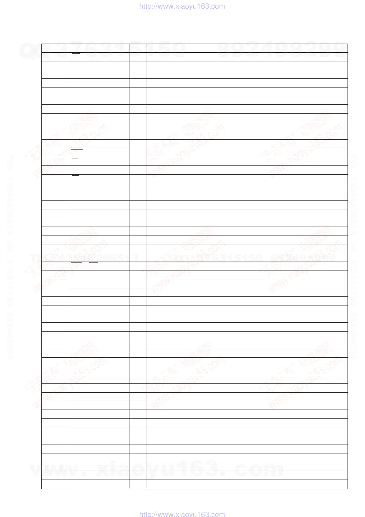
Pin No.
Pin Name
I/O
Function
79 CPA I/O Core priority access
80 DT0 O Data transmit
81 TCLK0 I/O transmit clock
82 TFS0 I/O Transmit frame sync
83 DR0 I Data receive
84 RCLK0 I/O Receive clock
85 RFS0 I/O Receive frame sync
86, 87 VDD – Power supply
88 GND – Ground
89 ADRCLK O Clock output reference
90 REDY O Host bus acknowledge
91 HBG I/O Host bus ground
92 CS I Chip select
93 RD I/O Memory read strobe
94 WR I/O Memory write strobe
95 GND – Ground
96 VDD – Power supply
97 GND – Ground
98 CLKIN I Clock in
99 ACK I/O Memory acknowledge
100 DMAG2 O DMA grant 2
101 DMAG1 O DMA grant 1
102 PAGE O DRAM page boundary
103 VDD – Power supply
104 to 109 BR6 to BR1 I/O Multiprocessing bus requests
110 GND – Ground
111 VDD – Power supply
112 GND – Ground
113 to 115 DATA47 to DATA45 I/O External bus data
116 VDD – Power supply
117 to 119 DATA44 to DATA42 I/O External bus data
120 GND – Ground
121 to 123 DATA41 to DATA39 I/O External bus data
124 VDD – Power supply
125 to 127 DATA38 to DATA36 I/O External bus data
128 GND – Ground
129 NC – Not used
130 to 132 DATA35 to DATA33 I/O External bus data
133, 134 VDD – Power supply
135 GND – Ground
136 to 138 DATA32 to DATA30 I/O External bus data
139 GND – Ground
140 to 142 DATA29 to DATA27 I/O External bus data
143, 144 VDD – Power supply
145 to 147 DATA26 to DATA24 I/O External bus data
148 GND – Ground
149 to 151 DATA23 to DATA21 I/O External bus data
152 VDD – Power supply
153 to 155 DATA20 to DATA18 I/O External bus data
156 GND – Ground
w
w
w
.
x
i
a
o
y
u
1
6
3
.
c
o
m
Q
Q
3
7
6
3
1
5
1
5
0
9
9
2
8
9
4
2
9
8
T
E
L
1
3
9
4
2
2
9
6
5
1
3
9
9
2
8
9
4
2
9
8
0
5
1
5
1
3
6
7
3
Q
Q
TEL 13942296513 QQ 376315150 892498299
TEL 13942296513 QQ 376315150 892498299
http://www.xiaoyu163.com
http://www.xiaoyu163.com
 Loading...