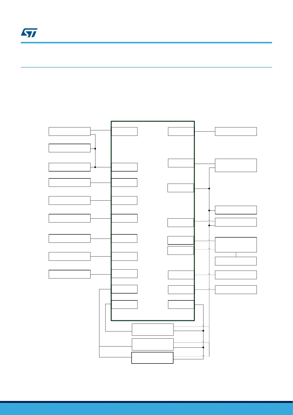
8 Hardware layout and configuration
The STM32H7B3I-DK Discovery kit is designed around the STM32H7B3LIH6QU target microcontroller packaged
in TFBGA225. The hardware block diagram, shown in Figure 3, illustrates the STM32H7B3LIH6QU connections
with the peripheral components. Figure 4 shows the location of the main components on the top side of the
Discovery board and Figure 5 shows the location of the main components on the bottom side of the Discovery
board.
Figure 3. STM32H7B3I-DK hardware block diagram
GPIO
FMC128-Mbit SDRAM
SWD
LCD and touch panel
OCSPI
Camera connector
Audio codec and
amplifier
microSD
TM
card
connector
3V3 / 1V8 Power supply
EXT_I2C connector
SDIO1
PWR
USART2
SPI2
USART1
RGB
DCMI
DFSDM
RTC / HSE
I2C4
UART4
SAI1
USB OTG connector
STLINK-V3E
32 KHz and
24 MHz crystals
512-Mbit Octo-SPI Flash
OTG HS
ARDUINO
®
connector
STMod+
TAG connector
SWD connector
Reset button
Audio connector
(5 MEMs microphones)
User LED
RSTn
STM32H7B3I
TFBGA225
Stereo jack with
microphone
Wi-Fi
®
I2S6
UM2569
Hardware layout and configuration
UM2569 - Rev 1
page 9/54