Pin Board function U5 smartcard interface pin
C7 I/O CARD DATA U5-11
C8 NC U5-12
S1 GND: CAR GND GND
S2 DETECT: CARD-Detect (LOW) U5-9
6.24 ADC/DAC
The STM32MP157F-EV1 provides some on-board analog-to-digital converters ADC and digital-to-analog
converters DAC:
•
2x ADC/DAC
• 2x Fast ADC
• 1x Slow ADC
6.24.1 ADC/DAC I/O interface
The STM32MP157FAA1 port PA4 may be configured to operate either as ADC input or as DAC output. PA4 is
routed to two-way headers
MB1263/JP11, to fetch signals to or from MB1263/JP11, or grounded by fitting a
jumper into MB1263/JP11. Same situation for PA5 and its related MB1263/JP10 header.
Parameters of the ADC/DAC low-pass filters formed with MB1263/R24, C31, R19 for PA4 and MB1263/R25, C32,
R20 for PA5 may be modified by replacing these components according to application requirements (Default
configuration is: R24/R19/R25/R20 = 0 Ω, C31/C32 not fitted).
6.24.2 Fast ADC
ANA0 may be configured as a fast ADC channel routed to MB1263/JP8. MB1263/SB6, closed by default, should
be opened.
ANA1 may be configured as a fast ADC channel routed to
MB1263/JP9. MB1263/SB7, closed by default, must be
opened.
Parameters of the low-pass filters formed with MB1263/R22, C29, and R17 for ANA0 and MB1263/R23, C30 and
R18 for ANA1 may be modified by replacing these components according to application requirements (Default
configuration is: R22/R17/R23/R18 = 0 Ω, C29/C30 not fitted).
6.24.3 Slow ADC
The port PF12 may be configured as slow ADC channel, routed to MB1263/JP7. MB1263/SB5, closed by default,
must be opened.
Parameters of the low-pass filters formed with
MB1263/R21, C28, and R16 may be modified to application
requirements (Default configuration is R21/R16=0 Ω, C28 not fitted).
The VREF+ terminal of STM32MP157FAA1 is used as reference voltage for both ADC and DAC. By default, it is
connected on board to VDDA through MB1263/R96, which may be removed to apply directly an external voltage
to VREF+ for specific purposes.
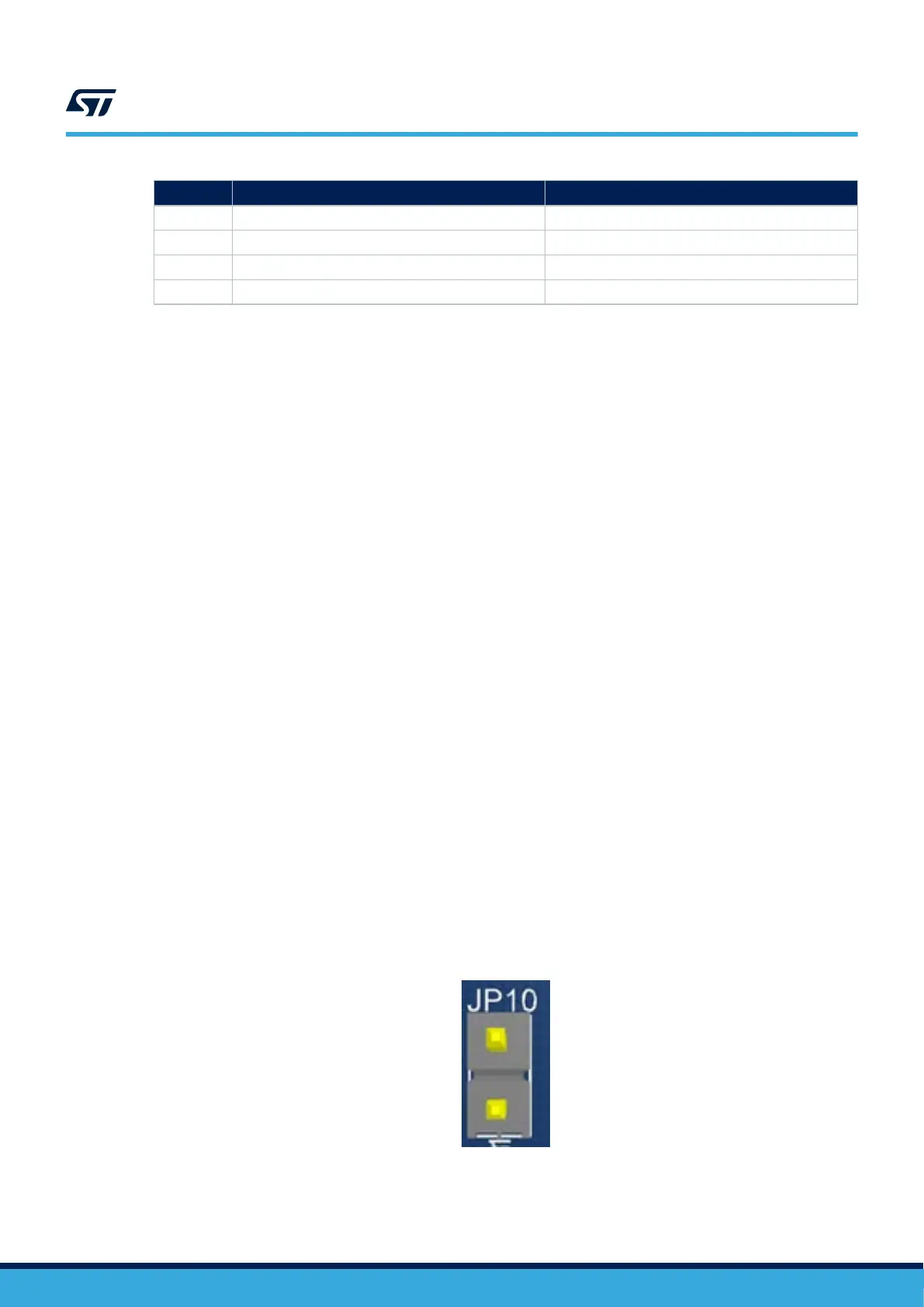
Figure 22 shows ADC/DAC connectors MB1263/JP7, JP8, JP9, JP10, and JP11.
Figure 22. ADC/DAC connectors MB1263/JP7, JP8, JP9, JP10, and JP11
UM2648
ADC/DAC
UM2648 - Rev 1
page 35/61