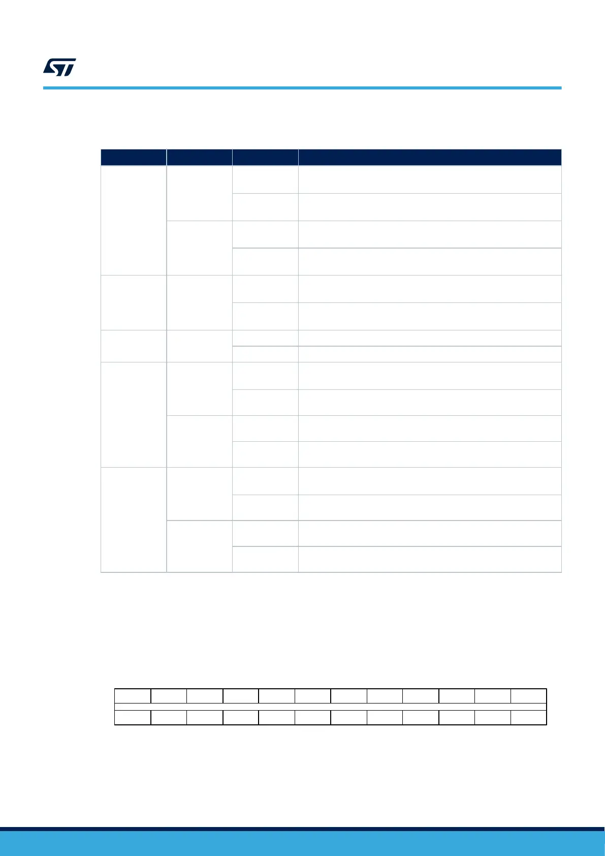
Table 13 describes the hardware configuration for the UCPD feature.
Table 13. Hardware configuration for the UCPD feature
I/O Solder bridge Setting
Configuration
(1)
PA15
SB42
OFF
PA15 Not connected to USB Type-C
®
port protection and used as
T_JTDI (optional configuration with SB39)
ON
PA15 connected to USB Type-C
®
port protection and NOT used as
T_JTDI
SB8
OFF
PA15 connected to USB Type-C
®
port protection and used as
UCPD_CC1
ON
PA15 directly connected to USB Type-C
®
connector. USB Type-C
®
port
protection is bypassed.
PB15 SB9
OFF
PB15 connected to USB Type-C
®
port protection and used as
UCPD_CC2
ON
PB15 directly connected to USB Type-C
®
connector. USB Type-C
®
port protection is bypassed.
PC2 SB6
ON PC2 used as VBUS_SENSE
OFF PC2 NOT used for UCPD. Can be used on Zio connector (SB53)
PB5
SB46
ON
IO UCPD_DBn connected to USB Type-C
®
port protection and
used as a dead battery feature
OFF
PB5 not used for UCPD_DBn can be used as SAI or SPI on ZIO
connector
JP8
ON
UCPD_DBCC1 connected to GND (only for internal UCPD debug
purpose)
OFF
UCPD_DBCC1 not connected to GND, can be used for Zio
connector
PB14
SB45
ON
IO UCPD_FLT connected to USB Type-C
®
port protection and used
as over‑voltage fault reporting to MCU
OFF
PB14 not used for UCPD_FLT can be used on the ST morpho
connector
JP7
ON
UCPD_DBCC2 connected to GND (only for internal UCPD debug
purpose)
OFF
UCPD_DBCC2 not connected to GND, can be used for the ST
morpho connector
1. The default configuration is shown in bold
6.11.3
USB Type-C
®
connector
shows the pinout of the USB Type-C
®
connector CN15.
Figure 15. CN15 USB Type-C
®
connector pinout
GND TX1+ TX1- VBUS CC1 D+ D- SBU1 VBUS RX2- RX2+ GND
GND RX1+ RX1- VBUS SBU2 D- D+ CC2 VBUS TX2- TX2+ GND
B12 B11 B10 B9 B8 B7 B6 B5 B4 B3 B2 B1
A1 A2 A3 A4 A5 A6 A7 A8 A9 A10 A11 A12
UM2861
USB Type-C® FS
UM2861 - Rev 2
page 30/49