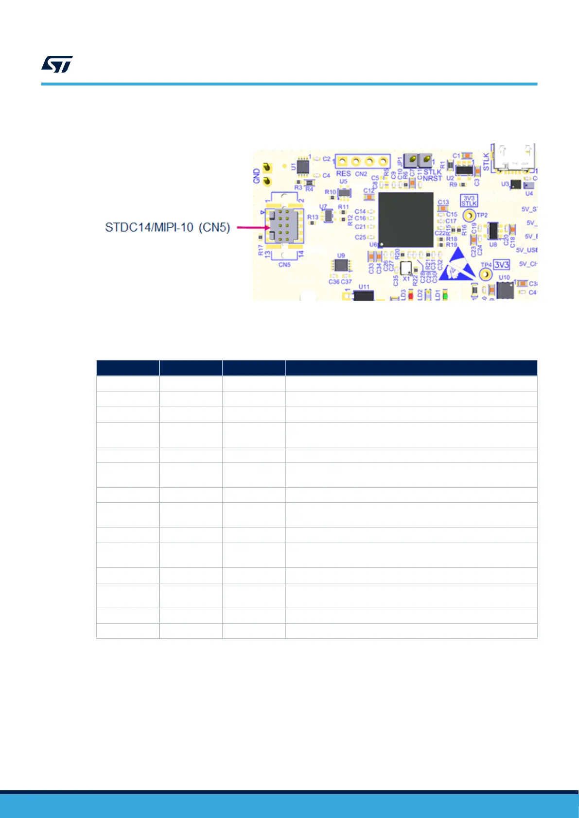
Figure 9 shows the CN5 STDC14/MIPI-10 connector.
Figure 9. CN5 STDC14/MIPI-10 debug connector
Table 7
describes the STDC14/MIPI-10 connector pinout.
Table 7. CN5 STDC14/MIPI-10 debug connector pinout
MIPI-10 pin STDC14 pin CN5 Function
- 1 NC Reserved
- 2 NC Reserved
1 3 VDD Target VDD
2 4 T_SWDIO
Target SWDIO using SWD protocol or target JTMS (T_JTMS) using
JTAG protocol
3 5 GND Ground
4 6 T_SWCLK
Target SWCLK using SWD protocol or target JTCK (T_JTCK) using
JTAG protocol
5 7 GND Ground
6 8 T_SWO
Target SWO using SWD protocol or target JTDO (T_JTDO) using JTAG
protocol (SB44 ON)
7 9 NC -
8 10 T_JTDI
Not used by SWD protocol, target JTDI (T_JTDI) using JTAG protocol,
only for external tools (SB39 OFF)
9 11 GNDDetect GND detect for plug indicator
10 12 T_NRST
Target NRST using SWD protocol or target JTMS (T_JTMS) using
JTAG protocol
- 13 T_VCP_RX Target RX used for VCP (with UART supporting bootloader)
- 14 T_VCP_TX Target TX used for VCP (with UART supporting bootloader)
Two SN74LVC2T45DCUT level shifters are used on VCP and SWD interface to offer a debug capability with 1V8
powered MCU. One level shifter is used for a signal from the MCU target (1V8) to STLINK-V3E (3V3).
• U1 used for T_VCP_TX signal
• U9 used for T_SWDIO and T_SWO signal
UM2861
Embedded STLINK-V3E
UM2861 - Rev 2
page 16/49