AN2752 Clock management
Doc ID 14651 Rev 3 13/42
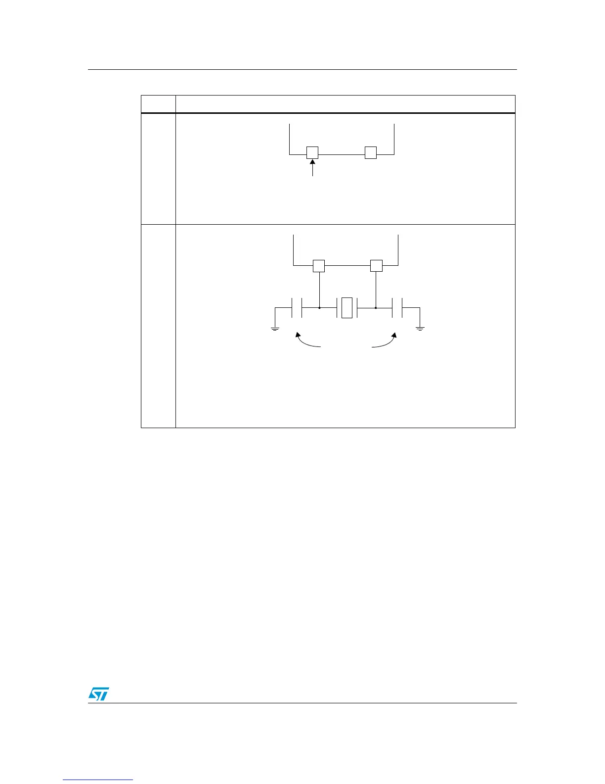
Figure 6. Clock sources
The values of the load capacitors C
L1
and C
L2
are heavily dependent on the crystal type and
frequency. The user can refer to the datasheet of the crystal manufacturer to select the
capacitances. For best oscillation stability C
L1
and C
L2
normally have the same value.
Typical values are in the range from below 20 pF up to 40 pF (cload: 10 … 20 pF). The
parasitic capacitance of the board layout also needs to be considered and typically adds a
few pF to the component values.
Recommendations
In the PCB layout all connections should be as short as possible. Any additional signals,
especially those that could interfere with the oscillator, should be locally separated from the
PCB area around the oscillation circuit using suitable shielding.
Hardware configuration
External clock
Frequency: 32 kHz … 24 MHz
Comparator hysteresis: 0.1 * V
DD
Caution: Without prescaler, a duty cycle of maximum 45/55% must be respected
Crystal/ceramic resonators
Frequency range: 1-24 MHz
Wake-up time: < 2 ms @ 24 MHz
Oscillation mode: Preferred fundamental
Output duty cycle: Max 55/45%
I/O’s: Standard I/O pins multiplexed with OSC
IN
and OSC
OUT
Cload: 10 … 20 pF
Maximum crystal power: 100 µW

 Loading...


