AN2752 Power supply
Doc ID 14651 Rev 3 7/42
2 Power supply
2.1 Power supply overview
The device can be supplied through a 3.0 V to 5.5 V external source. An on-chip power
management system provides the 1.8 V digital supply to the core logic, both in normal and
low power modes. It is also capable of detecting voltage drops, on both main external (3.3
V/5 V) and internal (1.8 V) supplies.
The device provides:
● One pair of pads V
DD
/V
SS
(3.3 V ± 0.3 V to 5 V ± 0.5 V) dedicated to the main regulator
ballast transistor supply.
● Two pairs of pads dedicated for V
DD_IO
/V
SS_IO
(3.3 V ± 0.3 V to 5 V ± 0.5 V), which are
used to power only the I/O’s. On 32-pin packages, only one pair is bonded.
Note: For V
DDIO
/V
SSIO
next to V
DD
/V
SS
, it is recommended to connect these two pairs together
and to use only one decoupling capacitance. The purpose is to ensure good noise immunity
by reducing the connection length between both supplies and also between V
DD
/V
DDIO
and
the capacitor.
● One pair of pads V
DDA
/V
SSA
(3.3 V ± 0.3 V to 5 V ± 0.5 V) dedicated to analog
functions. Refer to Section 3: Analog-to-digital converter (ADC) on page 10 for more
details.
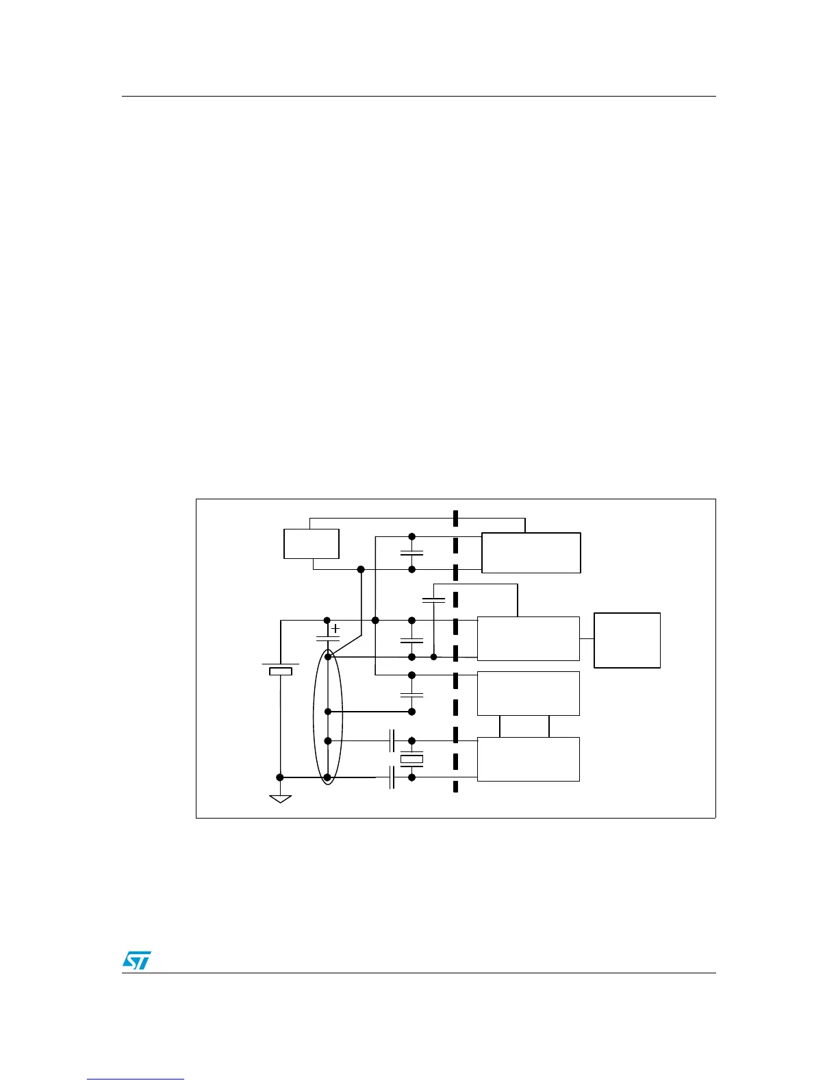
Figure 1. Power supply
Note: The capacitors must be connected as close as possible to the device supplies (especially
V
DD
in case of dedicated ground plane).
Placing a crystal/resonator on OSCIN/OSCOUT is optional. The resonator must be
connected as close as possible to the OSCIN and OSCOUT pins. The loading capacitance
ground must be connected as close as possible to V
SS
.

 Loading...


