TD350 Series VFD Function parameter list
-232-
Detailed parameter description
BIT5: S10 virtual terminal
BIT6: HDI3 virtual terminal
HDI3 terminal
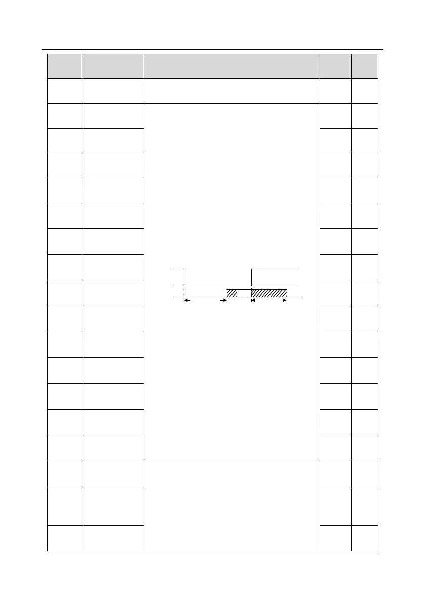
switch-on delay
These function codes define corresponding delay of
the programmable input terminals during level
variation from switch-on to switch-off .
Si electrical level
Si valid
invalid invalid
Switcn-on
delay
Switcn-off
delay
valid
Setting range: 0.000–50.000s
HDI3 terminal
switch-off delay
S5 terminal
switch-on delay
S6 terminal
switch-on delay
S7 terminal
switch-on delay
S8 terminal
switch-on delay
S9 terminal
switch-on delay
S10 terminal
switch-on delay
These function codes define the relation between
analog input voltage and corresponding set value of
analog input. When the analog input voltage
exceeds the range of max./min. input, the max.
input or min. input will be adopted during
calculation.
When analog input is current input, 0–20mA current
Corresponding
setting of lower
limit of AI3