3-25
The Save Memory Keep-Alive circuit maintains the con-
tents of the waveform "save" memory, RAM U350, during
periods that the oscilloscope power is turned off. A portion
of the circuit controls the chip-select input of the Save
RAM during normal operation. The keep-alive current to
RAM U350 is supplied by the charge stored in capacitor
C896. The large capacity value of C896 (one farad) pro-
vides sufficient energy to maintain the saved data in RAM
Save Memory Keep-Alive Supply
The RAM Buffer U352 allows data transfers to and
from the Waveform ~P RAM to take place. The buffer is
enabled by U580D when any of the Waveform ~P RAM
locations are addressed. Buffer direction is determined by
the WWR level.
RAM Buffer
Reading from and writing to the Waveform }.LPRAM
selected by the Address Decode circuit are controlled by
the WRD (waveform read) and WWR (waveform write) sig-
nals respectively.
The "coefficient" RAM, U432, provides further scratch-
pad storage.
The "command-temp" RAM, U440, provides temporary
scratch-pad storage of display calculations in process and
storage of commands to the Waveform ~P from the Sys-
tem }.LP.
The 8K-x-8-bit Save Memory, U350, is where the
Waveform ~P places acquired waveform data that should
be retained with power off. Waveforms stored is the Save
RAM are retained for at least five days at room tempera-
ture with the power off.
The Waveform ~P RAM resides in the Waveform ~P
address space and is used for storage and manipulation of
waveform-display data. The RAM consists of three
memories; the 8K-x-8-bit "Save Memory" RAM, the 2K-
x-8-bit "Command-temp" RAM, and the 2K-x-8-bit
"Coefficient" RAM.
Waveform ~p RAM
The outputs of U540 allow the accessing processor to
read the display status (SSREG), to read the two-byte
address of the last-acquired point (RDMARO and
RDMAR1), or to latch the present interrupt status
(COMREG). (See the "Display Status Register" and
"Interrupt Latch" descriptions for further explanation.)
The waveform memory-mapped I/O locations fall into
the next 4K block decoded by U570 (WMMIO). Addresses
falling within this block produce a LO on the WMMIO sig-
nal line and enable U540. Decoder U540 operates similarly
to U570 and uses address lines WAO-WA4 to produce its
various I/O enabling outputs. Address bits WA3 and WA4
are used as chip selects and cause the output of U540 to
fall into the eight locations immediately above those of
Decoder U884 (diagram 1) for System ~P memory-mapped
I/O.
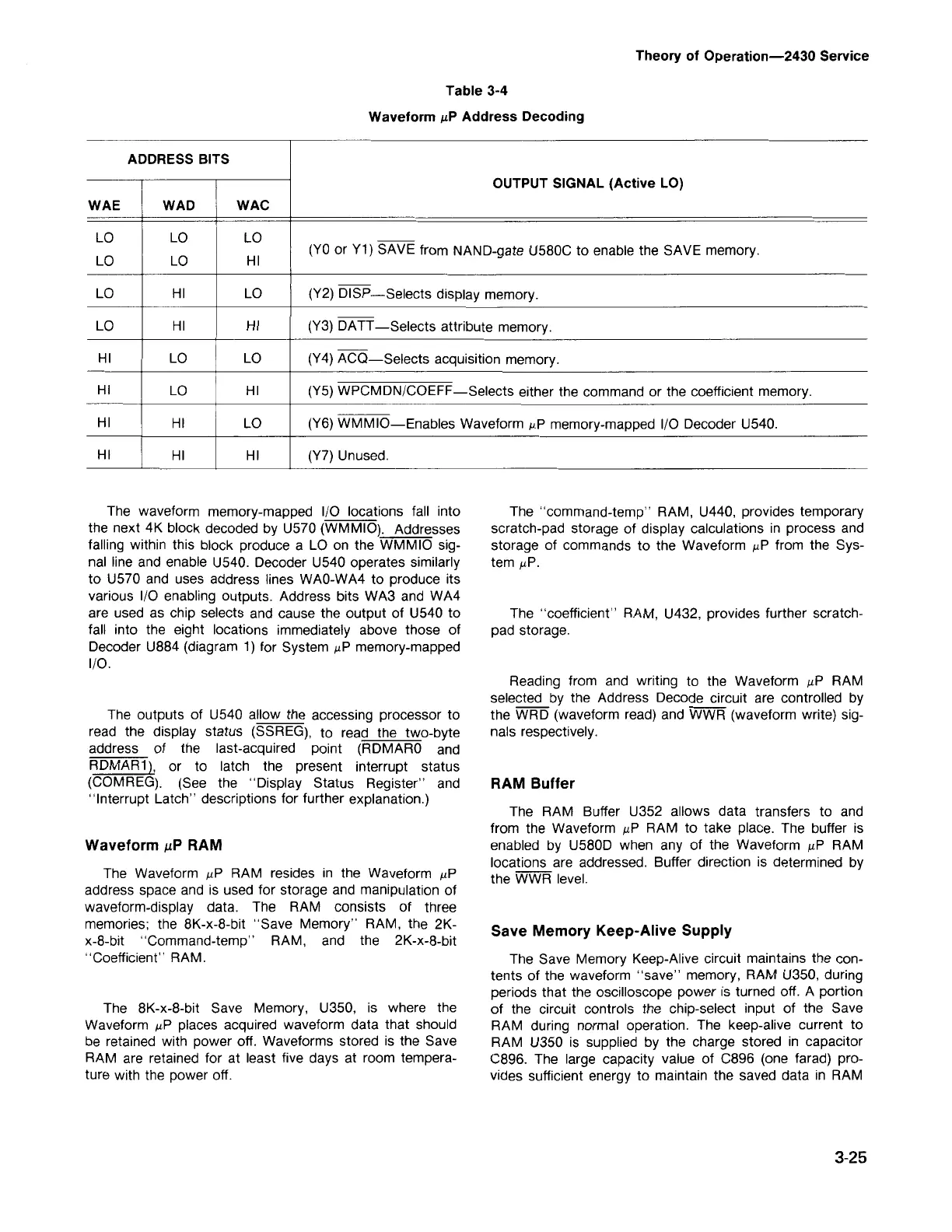
ADDRESS BITS
OUTPUT SIGNAL (Active LO)
WAE
WAD WAC
LO LO
LO
--
LO LO HI
(YOor Y1) SAVE from NAND-gate U580C to enable the SAVE memory.
LO
HI LO
--
(Y2) DISP-Selects display memory.
LO
--
HI HI
(Y3) DATT-Selects attribute memory.
--
HI
LO LO
(Y4) ACO-Selects acquisition memory.
HI
LO HI
(Y5) WPCMDN/COEFF-Selects either the command or the coefficient memory.
HI HI
LO
(Y6) WMMIO-Enables Waveform ~P memory-mapped I/O Decoder U540.
HI
HI HI
(Y7) Unused.
Table 3-4
Waveform ~P Address Decoding
Theory of Operation-2430 Service