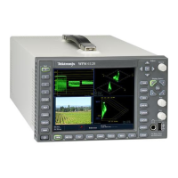
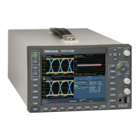
Theory of Operation
Option 3G/JIT
Option 3G adds 3 Gbps SDI input capability for the WFM7020 and WFM7120.
With the addition of option JIT (available for the WFM7120 only), 3 Gbps
operation is
extended to include jitter waveform display with readouts, and 3 Gbps
Loop-out Test Signal source capability. Since the Option 3G board is installed
in the Eye board slot, only one can be present. A ll non-EYE/PHY features and
functions are a vailable, including full HD and SD capabilities. Options 3G and
JIT provide the following features:
3 Gbps SDI input capability for 1080p 50, 59.94, 60; level A and level B
Down-converted (1080i) picture monitor outputs
Jitter readout
1
Jitter Meter
1
Jitter waveform display
1
Loop-out Test Signal Source
1
1
Requires Option JIT.
The hardware to support these features is contained on the 3G board, which is
installed in the center module slot. The Mezzanine board is removed when Option
3G is installed, so the SDI connectors move from the back panel lower right
quadrant to the center. See the 3G block diagram. (See Figure 2-3 on page 2-9.)
The Audio blocks are not shown in this block diagram but, if installed, still
connect as shown in the Main Block diagram. (See Figure 2-1 on page 2-2.)
Operation
Each SDI input signal is applied to a cable equalizer. The selected input is routed
to a re-clocker circuit, which extracts the clock and re-clocks the SDI signal.
The re-clocked SDI signal is applied to the 3 Gbps receiver/processor w ithin
the on-board FPGA. If the signal is recognized a s a valid 3 Gbps SDI stream,
then it is split into two 1.5 Gbps signals that are routed to the serial-to-parallel
receivers on the Main board. The FPGAs on the Main board combine the two
signals for measurement and display. If the selected input signal is not recognized
as a valid 3 Gbps SDI stream, then the equalized SDI A and SDI B signals are
routed directly to the main board, bypassing the 3Gbps processing. The Main
board then recognizes and process these signals if they are valid HD (1.5 Gbps) or
SD (270 Mbps) streams.
For 3 Gbps inputs, the recovered clock is divided by 40, filteredtoformasine
wave, and then digitized. This sine wave is sampled by an asynchronous clock
andpassedtothemainboardforprocessingbyFPGAs.Thesearraysproducethe
Jitter Waveform, Jitter Readout, and Jitter Thermometer.
The divided recovered clock also drives a PLL with selectable loop bandwidth,
providing the CLOCK OUT signal. An external oscilloscope viewing a copy of
the 3 Gbps input s ignal can be triggered from the CLOCK OUT signal in order to
display an eye diagram.
2–8 WFM6120, WFM7020, and WFM7120 Waveform Monitors Service Manual
 Loading...