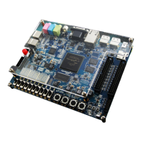
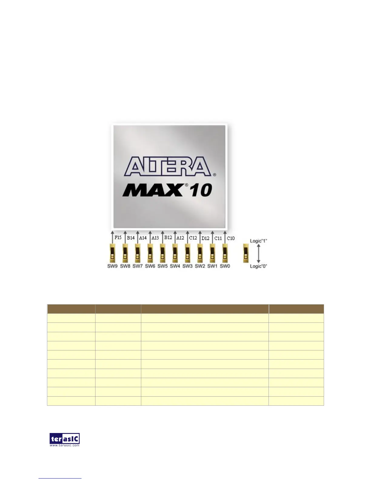
EasyManua.ls Logo

Terasic DE10-Lite - Page 27

Terasic DE10-Lite
75 pages
Print Icon
To Next Page IconTo Next Page
To Previous Page IconTo Previous Page
Loading...
DE10-Lite
User Manual
26
www.terasic.com
May 11, 2018
User-Defined Slide Switch
There are ten slide switches connected to FPGA on the board (See Figure 3-15). These switches are
used as level-sensitive data inputs to a circuit. Each switch is connected directly and individually to
a pin on the MAX 10 FPGA. When the switch is in the DOWN position (closest to the edge of the
board), it provides a low logic level to the FPGA, and when the switch is in the UP position it
provides a high logic level. Table 3-4 list the pin assignments of the user switches.
Figure 3-15 Connections between the slide switches and MAX 10 FPGA
Table 3-4 Pin Assignment of Slide Switches
Signal Name
FPGA Pin No.
Description
I/O Standard
SW0
PIN_C10
Slide Switch[0]
3.3-V LVTTL
SW1
PIN_C11
Slide Switch[1]
3.3-V LVTTL
SW2
PIN_D12
Slide Switch[2]
3.3-V LVTTL
SW3
PIN_C12
Slide Switch[3]
3.3-V LVTTL
SW4
PIN_A12
Slide Switch[4]
3.3-V LVTTL
SW5
PIN_B12
Slide Switch[5]
3.3-V LVTTL
SW6
PIN_A13
Slide Switch[6]
3.3-V LVTTL
SW7
PIN_A14
Slide Switch[7]
3.3-V LVTTL
SW8
PIN_B14
Slide Switch[8]
3.3-V LVTTL
SW9
PIN_F15
Slide Switch[9]
3.3-V LVTTL

Related product manuals