EVM Headers, Test Points, and Configuration
www.ti.com
50
SLOU489–August 2017
Submit Documentation Feedback
Copyright © 2017, Texas Instruments Incorporated
Hardware Configuration
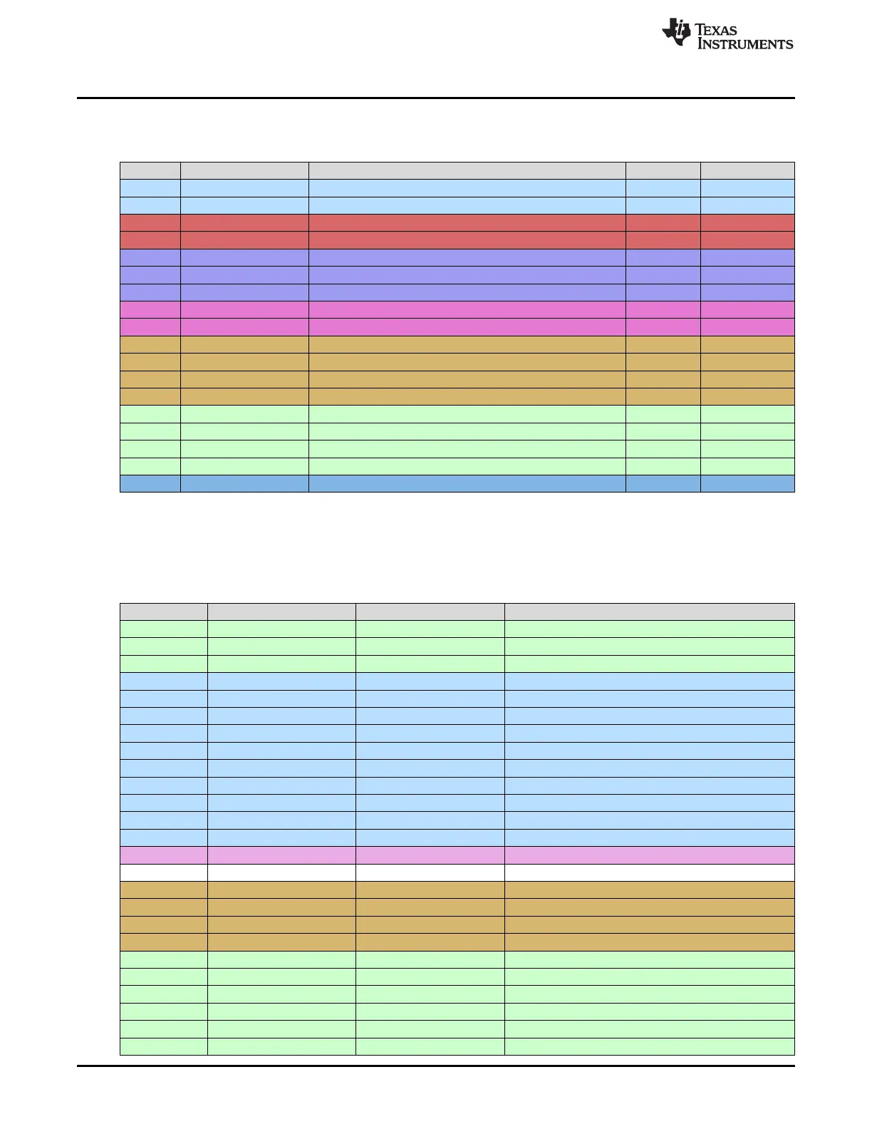
Table 1 lists the default header configurations and descriptions.
Table 1. Default Header Configuration Table Rev. A
Jumper Circuit Description Pin Numbers Selection
J63 Power Supply ±5V Input Power Connector – –
J64 USB/SPI SPI Signals Probe Point – –
J35 PDN PDN_Global – –
J36 PDN PDN_Fast – –
J41 ADC Clock OSC1 Xtal Power supply +3.3VD – 3.3V
J42 ADC Clock Clk source selector for SE Xtal or Diff 2-4,1-3 Differential
J40 ADC Clock Diff CLK Source selector, Ext Xfmr or LMK 3-5, 4-6 LMK CLK
J44 CW CLK 16x CLK Source Selector 3-5, 4-6 Ext
J45 CW CLK 1x CLK Source Selector 3-5, 4-6 Ext
J50 DTGC DTGC Digital Input Signals – –
J49 DTGC GND for Dig Input Signals – –
J60 DTGC CPLD JTAG Programming Header – –
J58 DTGC CPLD GPIO – –
J55 LMK LMK Chip Reset 1-2 –
J53 LMK LMK Supply for 125M Xtal 1-2 –
J57 LMK Power Supply for 40 MHz VCO 1-2 3.3V
J54 LMK Input Clk selector for Clkin1 1-2 125 MHz Xtal
J38 LNA TR Enable TR_EN 1-4 – –
C.1.2 EVM Testpoints
Table 2 lists all test points on the AFE5832 EVM and their purposes.
Table 2. EVM Rev. A Testpoints
Testpoint Circuit Label Testpoint Description
TP62-65, 69 GND GND Digital Ground Reference for EVM
TP31, 32 GND AGND Input Signal Ground Reference for EVM
TP66 GND DGND USB Ground Reference for EVM
T53 Power Supply +5V_IN +5V_IN
T54 Power Supply –5V_IN –5-V supply for Op-Amp circuitry
T59 Power Supply +1.8 VD AFE 1.8-V supply
TP67 Power Supply OPAMP- –5-V Supply for Op Amp circuitry
TP58 Power Supply 3.3 VD +3.3 VA
TP56 Power Supply AVDD_3.15 AFE analog supply for 3.15 V
TP68 Power Supply ODAMP+ +5-V Supply for Op Amp circuitry
TP57 Power Supply AVDD_1.9 AFE analog supply for 1.9-V
TP60 Power Supply +5V_SRC +5-V source for entire EVM
TP61 Power Supply –5VSS –5V Supply for CW Op Amp circuitry
TP1-30, 33, 34 Analog Inputs SMA_INPx Analog Input Channel 1-32
TP35 External Trigger TX_TRG TX_Trig input
TP38 DTGC None Ext TGC_Profile2 Input
TP36 DTGC None Ext TGC_Profile1 Input
TP37 DTGC TGC_SLP Ext TGC_Slope
TP39 DTGC TGC_UD Ext TGC_Up/Down
TP40,41 LMK Clock Circuit CP1,CP2 LMK Output CP1,CP2
TP42 LMK Clock Circuit None None
TP43 LMK Clock Circuit None None
TP44 LMK Clock Circuit None LMK ADC Clock to Dut P/N
TP45 LMK Clock Circuit None None
TP47 LMK Clock Circuit FPGA_CLK_OUT_P LMK ADC CLK to FPGA P