www.ti.com
EVM Headers, Test Points, and Configuration
51
SLOU489–August 2017
Submit Documentation Feedback
Copyright © 2017, Texas Instruments Incorporated
Hardware Configuration
Table 2. EVM Rev. A Testpoints (continued)
Testpoint Circuit Label Testpoint Description
TP48 LMK Clock Circuit None LMK VCXO output
TP46 LMK Clock Circuit None LMK Clock to CPLD
TP49 IC 0.5-V Source Bias None SRC_BIASO
TP50 IC 2.5-V Bias None BIAS_2P5E
TP51 IC BandGap Bias None BAND_GAPE
TP52 IC LNA Bias None LNA_IN_CME
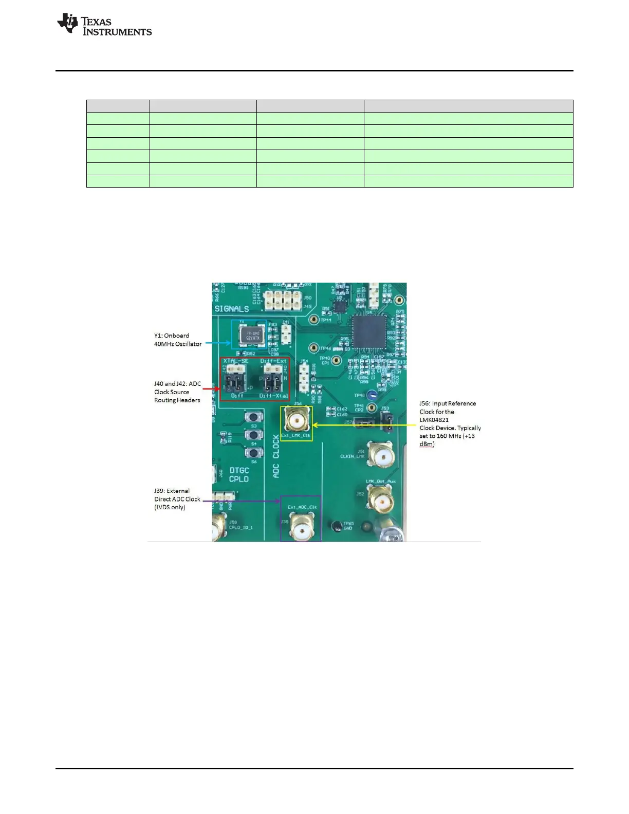
C.1.3 ADC Clock Source Configuration
The AFE clock input can be driven differentially (sine wave, LVPECL, or LVDS) or single-ended
(LVCMOS). The clock input of the device has an internal buffer and clock amplifier which is enabled or
disabled automatically, depending on the type of clock provided (auto-detect feature). Therefore, the EVM
allows for multiple clocking options.
Figure 61. EVM ADC Clock Source Configuration