EVM Headers, Test Points, and Configuration
www.ti.com
52
SLOU489–August 2017
Submit Documentation Feedback
Copyright © 2017, Texas Instruments Incorporated
Hardware Configuration
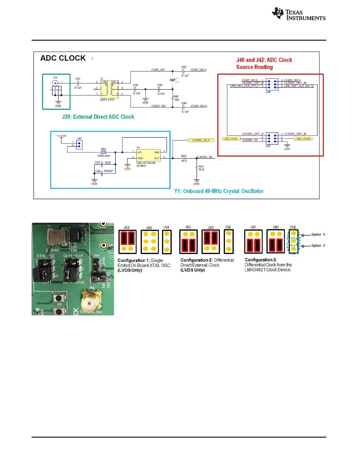
Figure 62. AFE EVM ADC Clock Source Configuration Schematic
Figure 63. EVM ADC Clock Source Configuration Examples
Configuration 1: To use the onboard single-ended crystal oscillator as the clock source for the AFE,
connect shunt jumpers for configuration 1 (as seen in Figure 63). Note: J41 powers the onboard oscillator
with 3.3 V, due to the power limitations of the FXO-HC735-40 low-jitter crystal oscillator. The
recommended ADC clock input for new designs is to use low-jitter square signals (LVCMOS levels, 1.8-V
amplitude).
Configuration 2 (LVDS Only): To use a direct external clock as the clock source for the AFE, connect
shunt jumpers for configuration 2 (as seen in Figure 63). Connect a single-ended external clock generator
to SMA J39. Set the clock source to an appropriate frequency, such as 10 MHz to 100 MHz, and +13-dBm
amplitude.