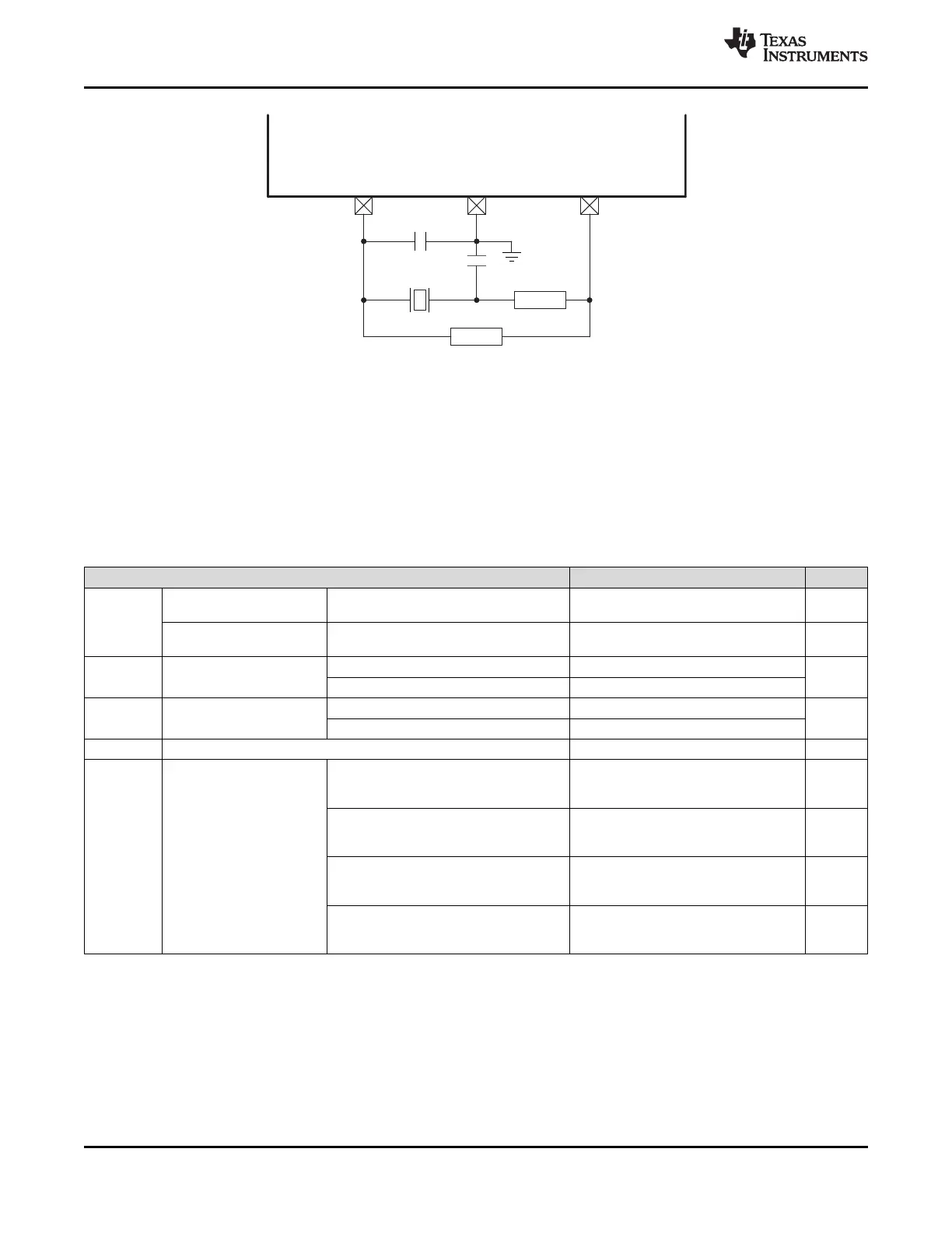
AM335x
XTALIN
VSS_OSC
XTALOUT
C
1
C
2
Optional R
d
Crystal
Optional R
bias
AM3359, AM3358, AM3357, AM3356, AM3354, AM3352
SPRS717H –OCTOBER 2011–REVISED MAY 2015
www.ti.com
A. Oscillator components (Crystal, C
1
, C
2
, optional R
bias
and R
d
) must be located close to the AM335x package.
Parasitic capacitance to the VSS_OSC and respective crystal circuit component grounds should be connected directly
to the nearest PCB digital ground (VSS).
B. C
1
and C
2
represent the total capacitance of the respective PCB trace, load capacitor, and other components
(excluding the crystal) connected to each crystal terminal. The value of capacitors C
1
and C
2
should be selected to
provide the total load capacitance, C
L
, specified by the crystal manufacturer. The total load capacitance is C
L
= [(C
1
×
C
2
) / (C
1
+ C
2
)] + C
shunt
, where C
shunt
is the crystal shunt capacitance (C
0
) specified by the crystal manufacturer plus
any mutual capacitance (C
pkg
+ C
PCB
) seen across the AM335x XTALIN and XTALOUT signals. For recommended
values of crystal circuit components, see Table 6-2.
Figure 6-9. OSC0 Crystal Circuit Schematic
Table 6-2. OSC0 Crystal Circuit Requirements
PARAMETER MIN TYP MAX UNIT
ƒ
xtal
Crystal parallel resonance Fundamental mode oscillation only 19.2, 24, MHz
frequency 25, or 26
Crystal frequency stability –50 50 ppm
and tolerance
(1)
C
shunt
≤ 5 pF 12 24
C
C1
C
1
capacitance pF
C
shunt
> 5 pF 18 24
C
shunt
≤ 5 pF 12 24
C
C2
C
2
capacitance pF
C
shunt
> 5 pF 18 24
C
shunt
Shunt capacitance 7 pF
ESR Crystal effective series ƒ
xtal
= 19.2 MHz, oscillator has nominal 54.4 Ω
resistance negative resistance of 272 Ω and worst-
case negative resistance of 163 Ω
ƒ
xtal
= 24 MHz, oscillator has nominal 48.0 Ω
negative resistance of 240 Ω and worst-
case negative resistance of 144 Ω
ƒ
xtal
= 25 MHz, oscillator has nominal 46.6 Ω
negative resistance of 233 Ω and worst-
case negative resistance of 140 Ω
ƒ
xtal
= 26 MHz, oscillator has nominal 45.3 Ω
negative resistance of 227 Ω and worst-
case negative resistance of 137 Ω
(1) Initial accuracy, temperature drift, and aging effects should be combined when evaluating a reference clock for this requirement.
108 Power and Clocking Copyright © 2011–2015, Texas Instruments Incorporated
Submit Documentation Feedback
Product Folder Links: AM3359 AM3358 AM3357 AM3356 AM3354 AM3352
 Loading...