AM3359, AM3358, AM3357, AM3356, AM3354, AM3352
SPRS717H –OCTOBER 2011–REVISED MAY 2015
www.ti.com
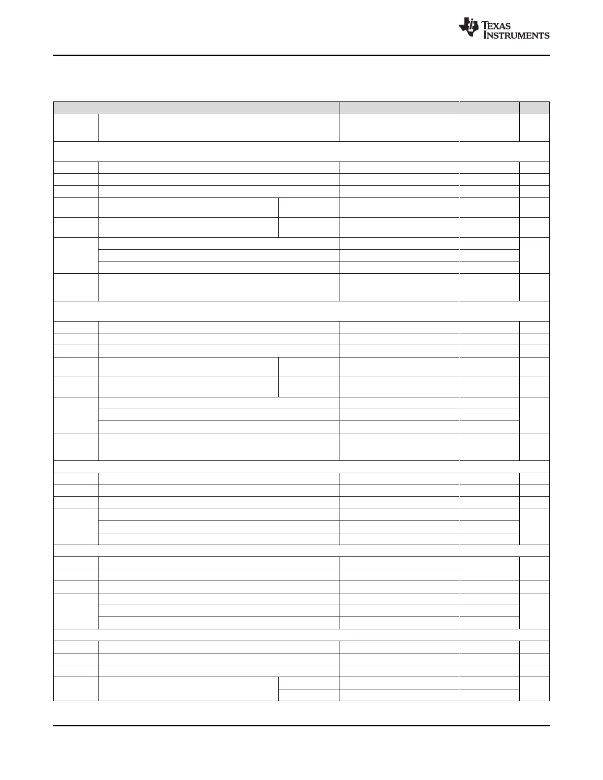
DC Electrical Characteristics
(1)
(continued)
over recommended ranges of supply voltage and operating temperature (unless otherwise noted)
PARAMETER MIN NOM MAX UNIT
I
OZ
Total leakage current through the terminal connection of a driver-receiver 10 µA
combination that may include a pullup or pulldown. The driver output is
disabled and the pullup or pulldown is inhibited.
ECAP0_IN_PWM0_OUT,UART0_CTSn,UART0_RTSn,UART0_RXD,UART0_TXD,UART1_CTSn,UART1_RTSn,UART1_RXD,UART1_TXD,I2C0_SDA,I2C0_
SCL,XDMA_EVENT_INTR0,XDMA_EVENT_INTR1,WARMRSTn,EXTINTn,TMS,TDO,USB0_DRVVBUS,USB1_DRVVBUS (VDDSHV6 = 1.8 V)
V
IH
High-level input voltage 0.65 × VDDSHV6 V
V
IL
Low-level input voltage 0.35 × VDDSHV6 V
V
HYS
Hysteresis voltage at an input 0.18 0.305 V
V
OH
High-level output voltage, driver enabled, pullup or I
OH
= 4 mA VDDSHV6 – 0.45 V
pulldown disabled
V
OL
Low-level output voltage, driver enabled, pullup or I
OL
= 4 mA 0.45 V
pulldown disabled
Input leakage current, Receiver disabled, pullup or pulldown inhibited 8
I
I
Input leakage current, Receiver disabled, pullup enabled –161 –100 –52 µA
Input leakage current, Receiver disabled, pulldown enabled 52 100 170
I
OZ
Total leakage current through the terminal connection of a driver-receiver 8 µA
combination that may include a pullup or pulldown. The driver output is
disabled and the pullup or pulldown is inhibited.
ECAP0_IN_PWM0_OUT,UART0_CTSn,UART0_RTSn,UART0_RXD,UART0_TXD,UART1_CTSn,UART1_RTSn,UART1_RXD,UART1_TXD,I2C0_SDA,I2C0_
SCL,XDMA_EVENT_INTR0,XDMA_EVENT_INTR1,WARMRSTn,EXTINTn,TMS,TDO,USB0_DRVVBUS,USB1_DRVVBUS (VDDSHV6 = 3.3 V)
V
IH
High-level input voltage 2 V
V
IL
Low-level input voltage 0.8 V
V
HYS
Hysteresis voltage at an input 0.265 0.44 V
V
OH
High-level output voltage, driver enabled, pullup or I
OH
= 4 mA VDDSHV6 – 0.45 V
pulldown disabled
V
OL
Low-level output voltage, driver enabled, pullup or I
OL
= 4 mA 0.45 V
pulldown disabled
Input leakage current, Receiver disabled, pullup or pulldown inhibited 18
I
I
Input leakage current, Receiver disabled, pullup enabled –243 –100 –19 µA
Input leakage current, Receiver disabled, pulldown enabled 51 110 210
I
OZ
Total leakage current through the terminal connection of a driver-receiver 18 µA
combination that may include a pullup or pulldown. The driver output is
disabled and the pullup or pulldown is inhibited.
TCK (VDDSHV6 = 1.8 V)
V
IH
High-level input voltage 1.45 V
V
IL
Low-level input voltage 0.46 V
V
HYS
Hysteresis voltage at an input 0.4 V
Input leakage current, Receiver disabled, pullup or pulldown inhibited 8
I
I
Input leakage current, Receiver disabled, pullup enabled –161 –100 –52 µA
Input leakage current, Receiver disabled, pulldown enabled 52 100 170
TCK (VDDSHV6 = 3.3 V)
V
IH
High-level input voltage 2.15 V
V
IL
Low-level input voltage 0.46 V
V
HYS
Hysteresis voltage at an input 0.4 V
Input leakage current, Receiver disabled, pullup or pulldown inhibited 18
I
I
Input leakage current, Receiver disabled, pullup enabled –243 –100 –19 µA
Input leakage current, Receiver disabled, pulldown enabled 51 110 210
PWRONRSTn (VDDSHV6 = 1.8 or 3.3 V)
(2)
V
IH
High-level input voltage 1.35 V
V
IL
Low-level input voltage 0.5 V
V
HYS
Hysteresis voltage at an input 0.07 V
V
I
= 1.8 V 0.1
I
I
Input leakage current µA
V
I
= 3.3 V 2
(2) The input voltage thresholds for this input are not a function of VDDSHV6.
90 Specifications Copyright © 2011–2015, Texas Instruments Incorporated
Submit Documentation Feedback
Product Folder Links: AM3359 AM3358 AM3357 AM3356 AM3354 AM3352

 Loading...