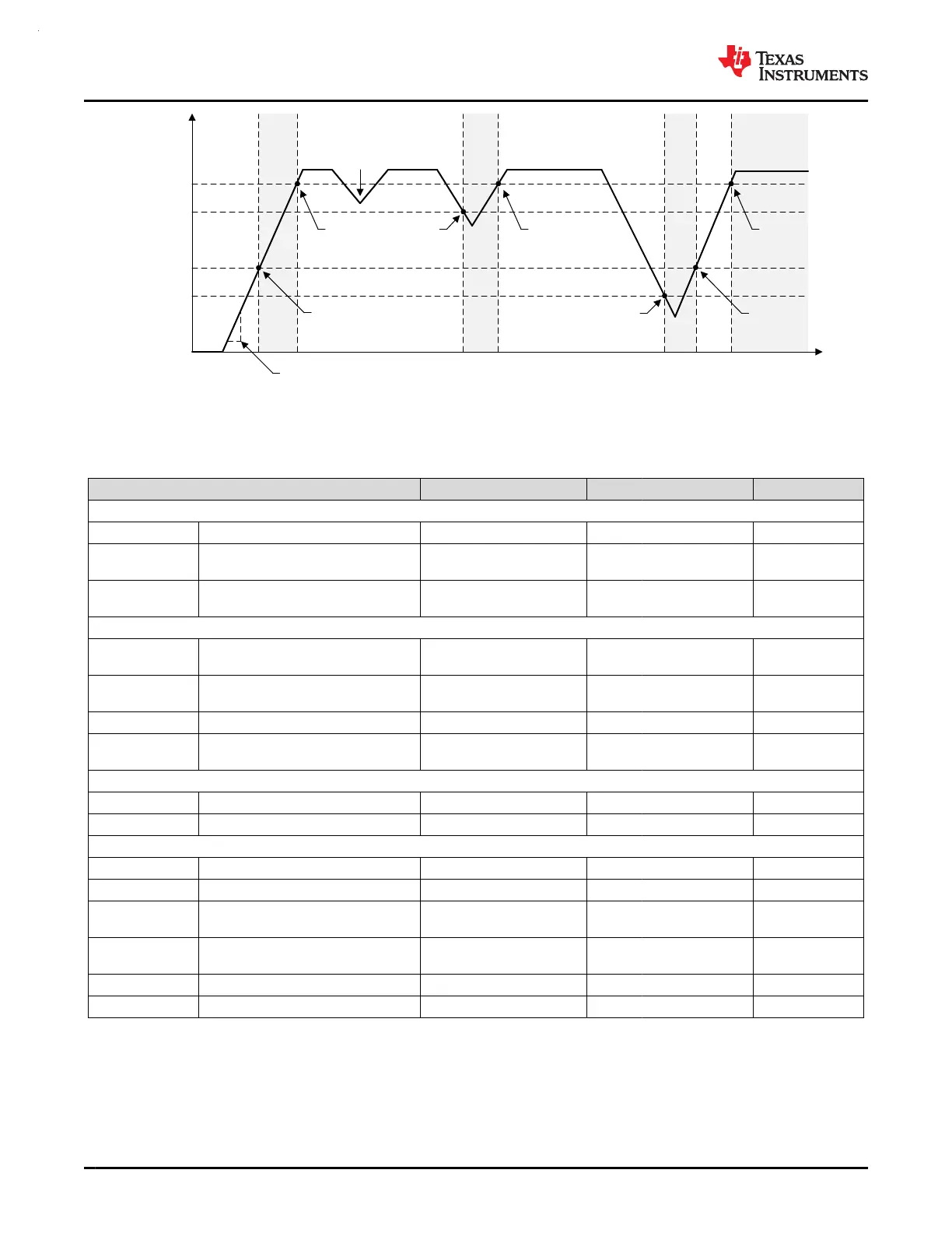
POR BOR Running RunningBOR POR BOR Running
Supply Voltage (VDD)
POR-
POR+
BOR0-
BOR0+
No reset
asserted
BOR
asserted
POR
asserted
BOR
released
POR
released
POR
released
BOR
released
Time (t)
POR/BOR levels are met
for specified |dVDD/dt|
BOR
released
Figure 7-1. Power Cycle POR/BOR Conditions
7.7 Flash Memory Characteristics
over operating free-air temperature range (unless otherwise noted)
PARAMETER TEST CONDITIONS MIN TYP MAX UNIT
Supply
VDD
PGM/ERASE
Program and erase supply voltage 1.62 3.6 V
IDD
ERASE
Supply current from VDD during erase
operation
Supply current delta 10 mA
IDD
PGM
Supply current from VDD during
program operation
Supply current delta 10 mA
Endurance
NWEC
(LOWER)
Erase/program cycle endurance (lower
32kB flash)
(1)
100 k cycles
NWEC
(UPPER)
Erase/program cycle endurance
(remaining flash)
(1)
10 k cycles
NE
(MAX)
Total erase operations before failure
(2)
802 k erase operations
NW
(MAX)
Write operations per word line before
sector erase
(3)
83 write operations
Retention
t
RET_85
Flash memory data retention -40°C <= Tj <= 85°C 60 years
t
RET_105
Flash memory data retention -40°C <= Tj <= 105°C 11.4 years
Program and Erase Timing
t
PROG (WORD, 64)
Program time for flash word
(4)
(6)
50 275 µs
t
PROG (SEC, 64)
Program time for 1kB sector
(5)
(6)
6.4 ms
t
ERASE (SEC)
Sector erase time
≤2k erase/program cycles,
T
j
≥25°C
4 20 ms
t
ERASE (SEC)
Sector erase time
≤10k erase/program cycles,
T
j
≥25°C
20 150 ms
t
ERASE (SEC)
Sector erase time <10k erase/program cycles 20 200 ms
t
ERASE (BANK)
Bank erase time <10k erase/program cycles 22 220 ms
(1) The lower 32kB flash address space supports higher erase/program endurance to enable EEPROM emulation applications. On
devices with <=32kB flash memory, the entire flash memory supports NWEC
(LOWER)
erase/program cycles.
(2) Total number of cumulative erase operations supported by the flash before failure. A sector erase or bank erase operation is
considered to be one erase operation.
(3) Maximum number of write operations allowed per word line before the word line must be erased. If additional writes to the same word
line are required, a sector erase is required once the maximum number of write operations per word line is reached.
(4) Program time is defined as the time from when the program command is triggered until the command completion interrupt flag is set in
the flash controller.
MSPM0G3507, MSPM0G3506, MSPM0G3505
SLASEX6A – FEBRUARY 2023 – REVISED JUNE 2023
www.ti.com
32 Submit Document Feedback
Copyright © 2023 Texas Instruments Incorporated
Product Folder Links: MSPM0G3507 MSPM0G3506 MSPM0G3505