8.16 DAC
The 12-bit buffered digital-to-analog converter (DAC) in these devices converts a digital input value into an
analog voltage to a buffered output channel and it supports the following key features:
• Up to 1-Msps output sampling rate
• 8-bit or 12-bit voltage-output resolution
• Self-calibration option for offset error correction
• Straight binary or twos-complement data format
• Integrated sample time generator for generation of predefined sampling rates
• Integrated FIFO and support DMA operation
• One hardware trigger from event fabric for conversion
• Programmable voltage reference options:
– Supply voltage (VDD)
– External reference voltage (VREF IO)
– Internal reference voltage (1.4V, 2.5V)
For more information about device analog connections, see Section 8.30.
For more details, see the DAC chapter of the MSPM0 G-Series 80-MHz Microcontrollers Technical Reference
Manual.
8.17 OPA
The zero-drift op amps (OPAs) in these devices, OPA0 and OPA1, are chopper stabilized operational amplifiers
with rail-to-rail input/output and a programmable gain stage feedback loop.
The OPA peripherals support the following key features:
• Software-selectable zero-drift chopper stabilization for improved accuracy and drift performance
• Factory trimming to remove offset error
• Burnout current source (BCS) integrated to monitor sensor health
• Programmable gain amplifier (PGA) up to 32x
The OPA features configurable input muxes P-MUX, N-MUX, and M-MUX to support various analog signal chain
amplifier configurations that include general purpose, inverting, noninverting, unity gain, cascade, noninverting
cascade, difference, and more. The following tables list the input channel mapping for each OPA.
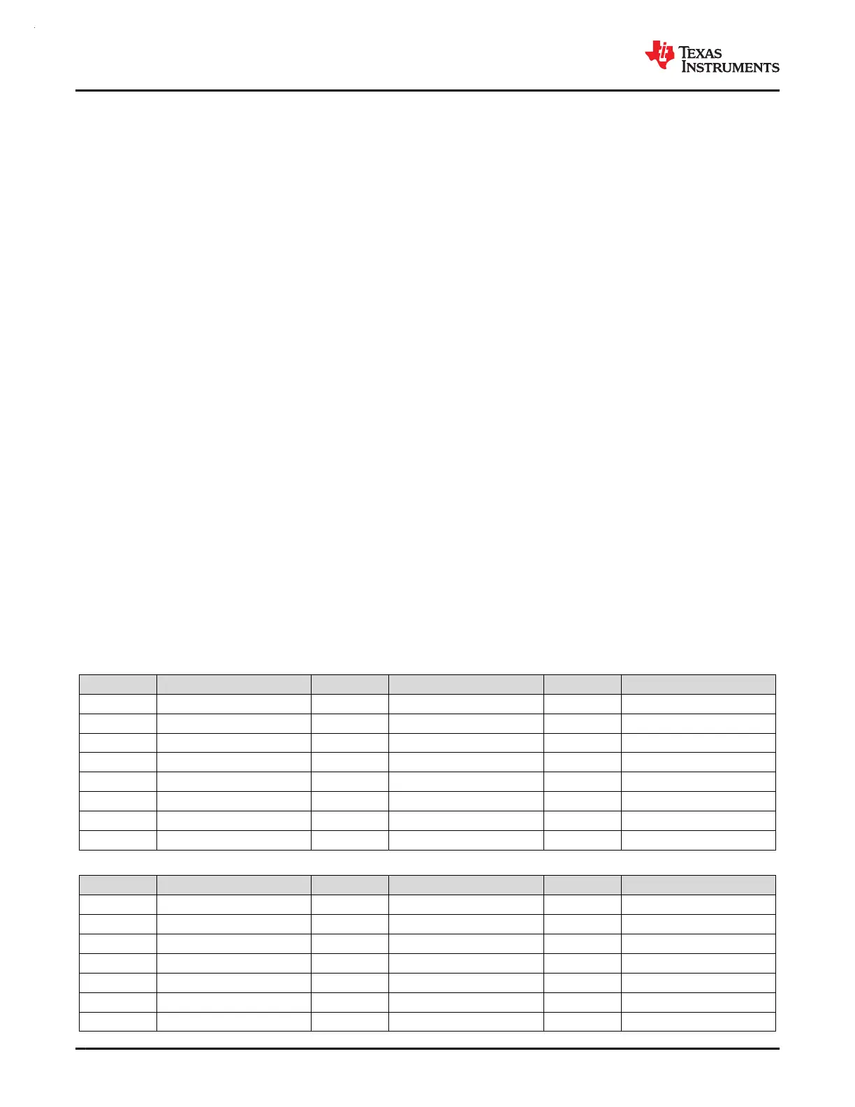
Table 8-12. OPA0 Input Channel Mapping
PSEL P-MUX INPUTS NSEL N-MUX INPUTS MSEL M-MUX INPUTS
0x0 Open 0x0 Open 0x0 Open
0x1 OPA0_IN0+ 0x1 OPA0_IN0- 0x1 OPA0_IN1-
0x2 OPA0_IN1+ 0x2 OPA0_IN1- 0x2 GND
0x3 DAC_OUT / OPA0_IN2+
(1)
0x3 OPA1_RBOT 0x3 DAC_OUT / OPA0_IN2+
(1)
0x4 DAC8.0_OUT 0x4 RTAP 0x4 OPA1_RTOP
0x5 VREF 0x5 RTOP
0x6 OPA1_RTOP
0x7 GPAMP Output
Table 8-13. OPA1 Input Channel Mapping
PSEL P-MUX INPUTS NSEL N-MUX INPUTS MSEL M-MUX INPUTS
0x0 Open 0x0 Open 0x0 Open
0x1 OPA1_IN0+ 0x1 OPA1_IN0- 0x1 OPA1_IN1-
0x2 OPA1_IN1+ 0x2 OPA1_IN1- 0x2 GND
0x3 DAC_OUT / OPA1_IN2+
(1)
0x3 OPA0_RBOT 0x3 DAC_OUT / OPA1_IN2+
(1)
0x4 DAC8.1_OUT 0x4 RTAP 0x4 OPA0_RTOP
0x5 VREF 0x5 RTOP
0x6 OPA0_RTOP
MSPM0G3507, MSPM0G3506, MSPM0G3505
SLASEX6A – FEBRUARY 2023 – REVISED JUNE 2023
www.ti.com
64 Submit Document Feedback
Copyright © 2023 Texas Instruments Incorporated
Product Folder Links: MSPM0G3507 MSPM0G3506 MSPM0G3505