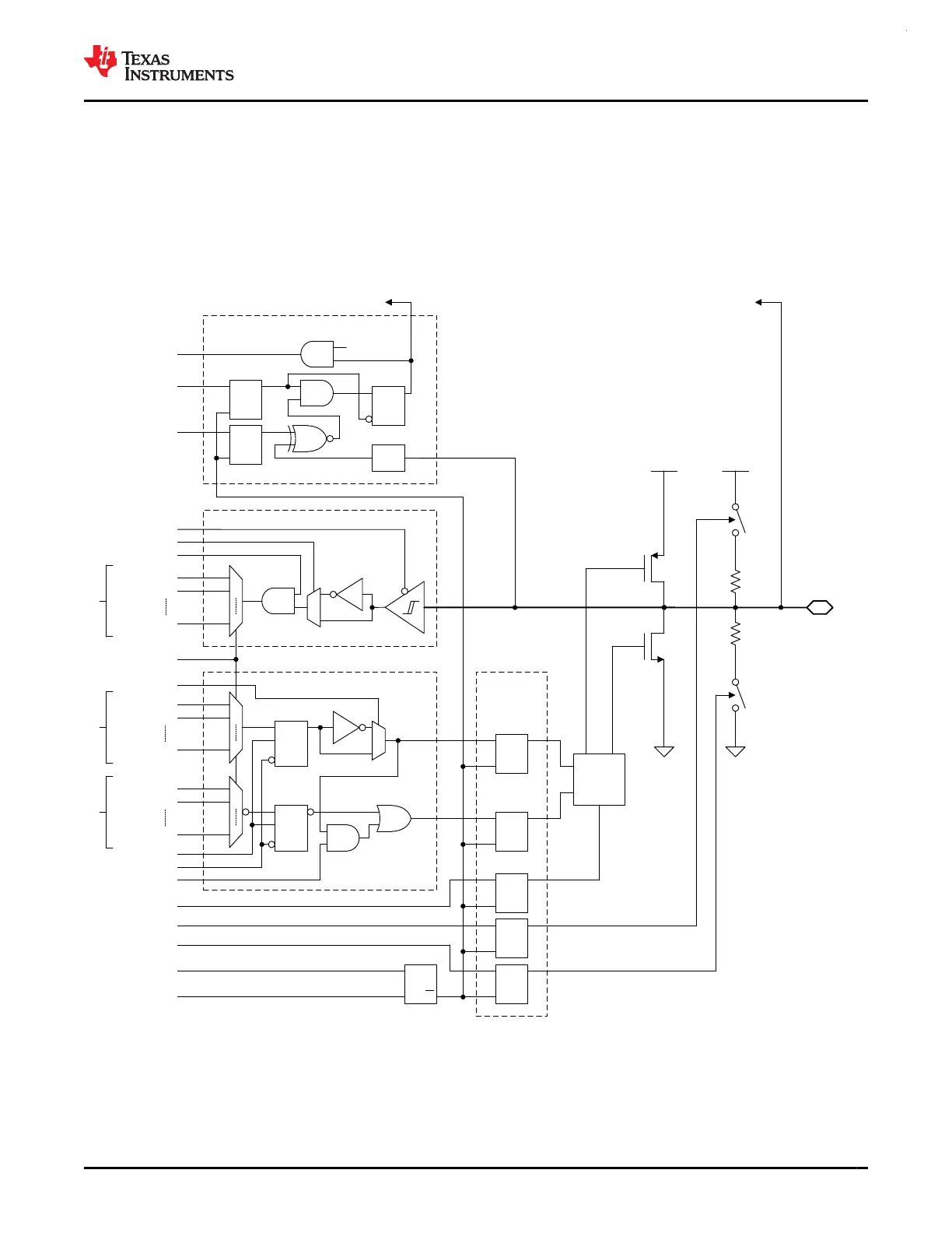
8.31 Input/Output Diagrams
The IOMUX manages the selection of which peripheral function is to be used on a digital IO. It also provides the
controls for the output driver, input path, and the wake-up logic for wakeup from SHUTDOWN mode. For more
information, refer to the IOMUX section of the MSPM0 G-Series 80-MHz Microcontrollers Technical Reference
Manual.
The mixed-signal IO pin slice diagram for a full featured IO pin is shown in Figure 8-2. Not all pins will have
analog functions, wake-up logic, drive strength control, and pullup or pulldown resistors available. See the
device-specific data sheet for detailed information on what features are supported for a specific pin.
R
PULLUP
VDDIO
PC
R
PULLDOWN
VSS
Z1
HYSTEN
INENA
0
1
15
Unassigned
Peripheral 01
Peripheral 15
0
1
15
Unassigned
Peripheral 01
Peripheral 15
PF
SHUTDOWN Wakeup
WCOMP
VSS
VDDIO
DRV
Glitch
Filter
WUEN
Wake to PMCU
IO pin
SHUTDOWN
D Q
EN
D Q
EN
D Q
EN
S Q
R
WAKESTATE
Input Logic
Output Logic
PIPU
PIPD
To analog peripheral function(s)
D Q
EN
D Q
EN
D Q
EN
D Q
EN
D Q
EN
SHUTDOWN
Latches
Pullup enable
Pulldown enable
1
0
INV
1
0
INV
PMOS
NMOS
DIN
DOUT
0
1
15
Unassigned
Peripheral 01
Peripheral 15
Hi-Z
D Q
EN
Hi-Z Output Mux Output Mux Input Mux
Driver
Logic
Drive strength
NMOS Control
PMOS Control
S
R
RELEASE
Q
RSTN
RSTN
PF != 0
PC
5V tolerant open drain IO (ODIO)
does not have PMOS control and
pull-up resistor
Figure 8-2. Superset Input/Output Diagram
www.ti.com
MSPM0G3507, MSPM0G3506, MSPM0G3505
SLASEX6A – FEBRUARY 2023 – REVISED JUNE 2023
Copyright © 2023 Texas Instruments Incorporated
Submit Document Feedback
71
Product Folder Links: MSPM0G3507 MSPM0G3506 MSPM0G3505