(3) Analog power supply monitor. Analog input on channel 15 is disconnected and is internally connected to the voltage divider which is
VDD/3.
7.12.2 Switching Characteristics
over recommended ranges of supply voltage and operating free-air temperature (unless otherwise noted)
PARAMETER TEST CONDITIONS MIN TYP MAX UNIT
f
ADCCLK
ADC clock frequency 4 48 MHz
t
ADC trigger
Software trigger minimum width 3
ADCCLK
cycles
t
Sample
Sampling time without OPA 12-bit mode, R
S
= 50Ω, C
pext
= 10pF 62.5 ns
t
Sample_PGA
Sampling time with OPA
(1)
12-bit mode
GBW = 0x1, PGA gain = x1 0.25 µs
GBW = 0x1, PGA gain = x32 2 µs
t
Sample_DAC
Sampling time with DAC as input
(2)
0.5 µs
t
Sample_GPAMP
Sampling time with GPAMP 1.88 µs
t
Sample_SupplyMon
Sample time with Supply Monitor (VDD/3) 2.38 µs
(1) Only applies for devices with OPA
(2) Only applies for devices with DAC
7.12.3 Linearity Parameters
over recommended ranges of supply voltage and operating free-air temperature (unless otherwise noted), all TYP values are
measured at 25℃ and all linearity parameters are measured using 12-bit resolution mode (unless otherwise noted)
(1)
PARAMETER TEST CONDITIONS MIN TYP MAX UNIT
EI Integral linearity error (INL) External reference
(2)
External reference
(2)
-2.0 +2.0 LSB
E
D
Differential linearity error (DNL)
Guaranteed no missing codes
External reference
(2)
External reference
(2)
-1.0 +1.0 LSB
E
O
Offset error
External reference
(2)
-3 3 mV
Internal reference, V
R+
= VREF = 2.5V -3 3 mV
E
G
Gain error External reference
(2)
-3 3 LSB
(1) Total Unadjusted Error (TUE) can be calculated from E
I
, E
O
, and E
G
using the following formula: TUE = √( E
I
2
+ |E
O
|
2
+ E
G
2
)
Note: You must convert all of the errors into the same unit, usually LSB, for the above equation to be accurate
(2) All external reference specifications are measured with V
R+
= VREF+ = VDD and V
R-
= VSS = 0V, and HW Averaging feature will only
be supported since PG2.0.
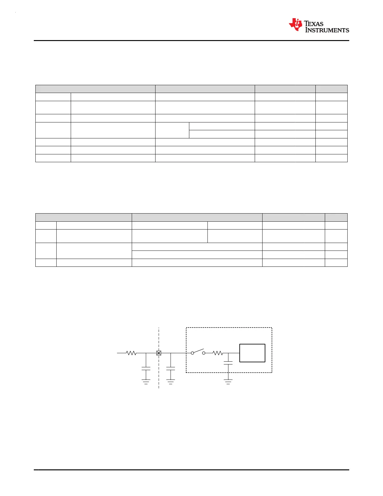
7.12.4 Typical Connection Diagram
V
in
R
par
C
par
R
in
C
I
ADC Model
C
S/H
S1
Device
Boundary
12-bit SAR
Converter
Figure 7-4. ADC Input Network
1. Refer to ADC Electrical Characteristics for the values of R
in
and C
S/H
2. Refer to Digital IO Electrical Characteristics for the value of C
I
3. C
par
and R
par
represent the parasitic capacitance and resistance of the external ADC input circuitry
Use the following equations to solve for the minimum sampling time (T) required for an ADC conversion:
1. Tau = (R
par
+ R
in
)* C
S/H
+ R
par
*(C
par
+ C
I
)
2. K= ln(2
n
/Settling error) – ln((C
par
+ C
I
)/C
S/H
)
MSPM0G3507, MSPM0G3506, MSPM0G3505
SLASEX6A – FEBRUARY 2023 – REVISED JUNE 2023
www.ti.com
40 Submit Document Feedback
Copyright © 2023 Texas Instruments Incorporated
Product Folder Links: MSPM0G3507 MSPM0G3506 MSPM0G3505