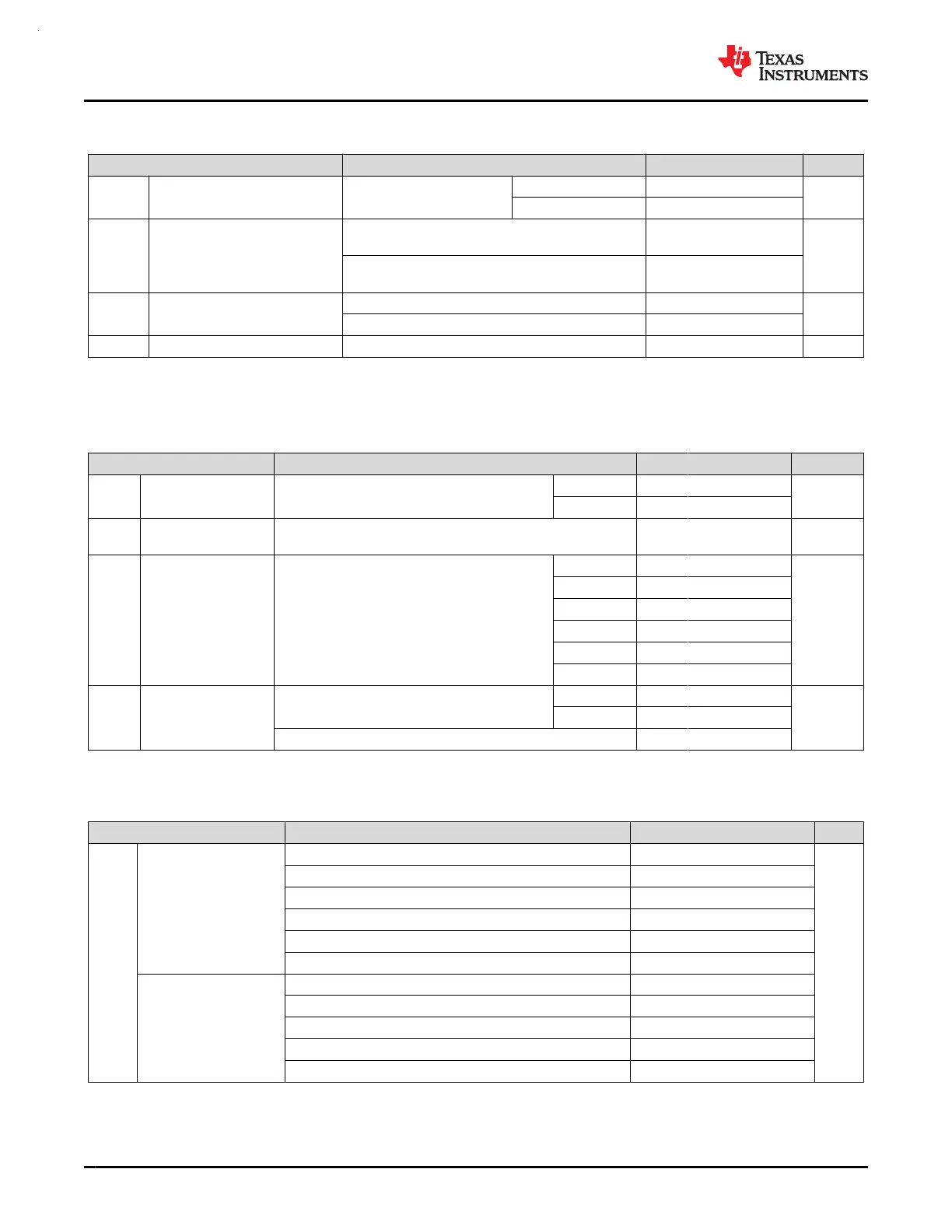
7.18.1 Electrical Characteristics (continued)
over recommended ranges of supply voltage and operating free-air temperature (unless otherwise noted)
PARAMETER TEST CONDITIONS MIN TYP MAX UNIT
SR Slew rate
Noninverting, unity gain, C
L
=
40 pF
GBW = 0x0 1.3
V/µs
GBW = 0x1 4.9
THDN Total harmonic distortion + noise
Noninverting, unity gain, GBW = 0x0, f = 1.5kHz,
Integration BW = 100kHz
0.0034
%
Noninverting, unity gain, GBW = 0x1, f = 6kHz,
Integration BW = 100kHz
0.004
I
Load
Output load current
GBW = 0x0 ±9
mA
GBW = 0x1 ±30
C
Load
Output load capacitance 40 pF
(1) R
in
here means the input resistance of mux in OPA.
7.18.2 Switching Characteristics
over recommended ranges of supply voltage and operating free-air temperature (unless otherwise noted)
PARAMETER TEST CONDITIONS MIN TYP MAX UNIT
t
EN
OPA enable time
ENABLE = 0x0 to 0x1, Bandgap reference ON,
0.1%, Noninverting, unity gain
GBW = 0x0 7.3 12
µs
GBW = 0x1 4.4 6
t
disable
OPA disable time 4
ULPCLK
cycles
f
CHOP
OPA Chopping
Frequency
CHOP = 0x1 or 0x2
GAIN = 0x0 125
kHz
GAIN = 0x1 62.5
GAIN = 0x2 31.25
GAIN = 0x3 15.625
GAIN = 0x4 7.8
GAIN = 0x5 3.9
t
SETTLE
OPA settling time
C
L
= 40 pF, Vstep = 0.3V to VDD-0.3V, 0.1%,
ENABLE = 0x1, Noninverting, unity gain
GBW = 0x0 2.5 9
µsGBW = 0x1 1.3 5
Change in op-amp configuration (CFG) 25 50
7.18.3 PGA Mode
over recommended ranges of supply voltage and operating free-air temperature (unless otherwise noted)
PARAMETER TEST CONDITIONS MIN TYP MAX UNIT
G
non- inverting gain
GAIN = 0x0 –0.05% 1 +0.05%
V/V
GAIN = 0x1 –0.6% 2 +0.6%
GAIN = 0x2 –0.8% 4 +0.8%
GAIN = 0x3 –1% 8 +1%
GAIN = 0x4 –1.5% 16 +1.5%
GAIN = 0x5 –2.6% 32 +2.6%
inverting gain
GAIN = 0x1 –0.8% –1 +0.8%
GAIN = 0x2 –1.0% –3 +1.0%
GAIN = 0x3 –1.2% –7 1.2%
GAIN = 0x4 –1.5% –15 1.5%
GAIN = 0x5 –2.7% –31 2.7%
MSPM0G3507, MSPM0G3506, MSPM0G3505
SLASEX6A – FEBRUARY 2023 – REVISED JUNE 2023
www.ti.com
46 Submit Document Feedback
Copyright © 2023 Texas Instruments Incorporated
Product Folder Links: MSPM0G3507 MSPM0G3506 MSPM0G3505