N2HET1 N2HET2
ePWM1
2VCLK4cycles
PulseStrength
ePWM1_SYNCI
SYNCI
EXT_LOOP_SYNCN2HET1_LOOP_SYNC
ePWM1_SYNCI_SYNCED
ePWM1_SYNCI_FILTERED
PINMMR47[8,9,10]
PINMMR36[25]
RM46L852
SPNS185 –SEPTEMBER 2012
www.ti.com
5.1.1 ePWM Clocking and Reset
Each ePWM module has a clock enable (EPWMxENCLK). When SYS_nRST is active low, the clock
enables are ignored and the ePWM logic is clocked so that it can reset to a proper state. When
SYS_nRST goes in-active high, the state of clock enable is respected.
Table 5-1. ePWMx Clock Enable Control
ePWM Module Instance Control Register to Enable Clock Default Value
ePWM1 PINMMR37[8] 1
ePWM2 PINMMR37[16] 1
ePWM3 PINMMR37[24] 1
ePWM4 PINMMR38[0] 1
ePWM5 PINMMR38[8] 1
ePWM6 PINMMR38[16] 1
ePWM7 PINMMR38[24] 1
The default value of the control registers to enable the clocks to the ePWMx modules is 1. This means
that the VCLK4 clock connections to the ePWMx modules are enabled by default. The application can
choose to gate off the VCLK4 clock to any ePWMx module individually by clearing the respective control
register bit.
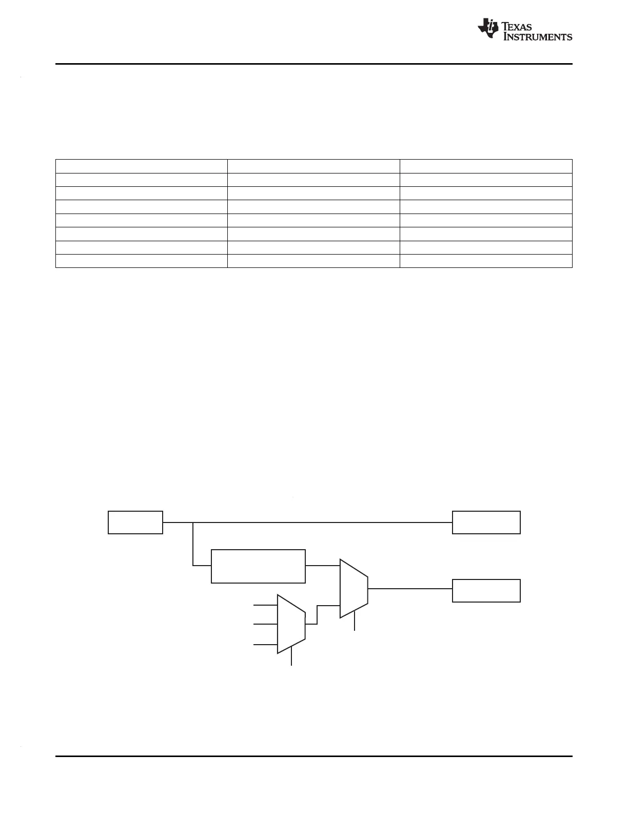
5.1.2 Synchronization of ePWMx Time Base Counters
A time-base synchronization scheme connects all of the ePWM modules on a device. Each ePWM
module has a synchronization input (EPWMxSYNCI) and a synchronization output (EPWMxSYNCO). The
input synchronization for the first instance (ePWM1) comes from an external pin. Figure 5-1 shows the
synchronization connections for all the ePWMx modules. Each ePWM module can be configured to use or
ignore the synchronization input. Refer to the ePWM chapter in the device Technical Reference Manual
for more information.
5.1.3 Synchronizing all ePWM Modules to the N2HET1 Module Time Base
The connection between the N2HET1_LOOP_SYNC and SYNCI input of ePWM1 module is implemented
as shown in Figure 5-2.
Figure 5-2. Synchronizing Time Bases Between N2HET1, N2HET2 and ePWMx Modules
118 Peripheral Information and Electrical Specifications Copyright © 2012, Texas Instruments Incorporated
Submit Documentation Feedback