RM46L852
SPNS185 –SEPTEMBER 2012
www.ti.com
6.3 Device Identification
6.3.1 Device Identification Code Register
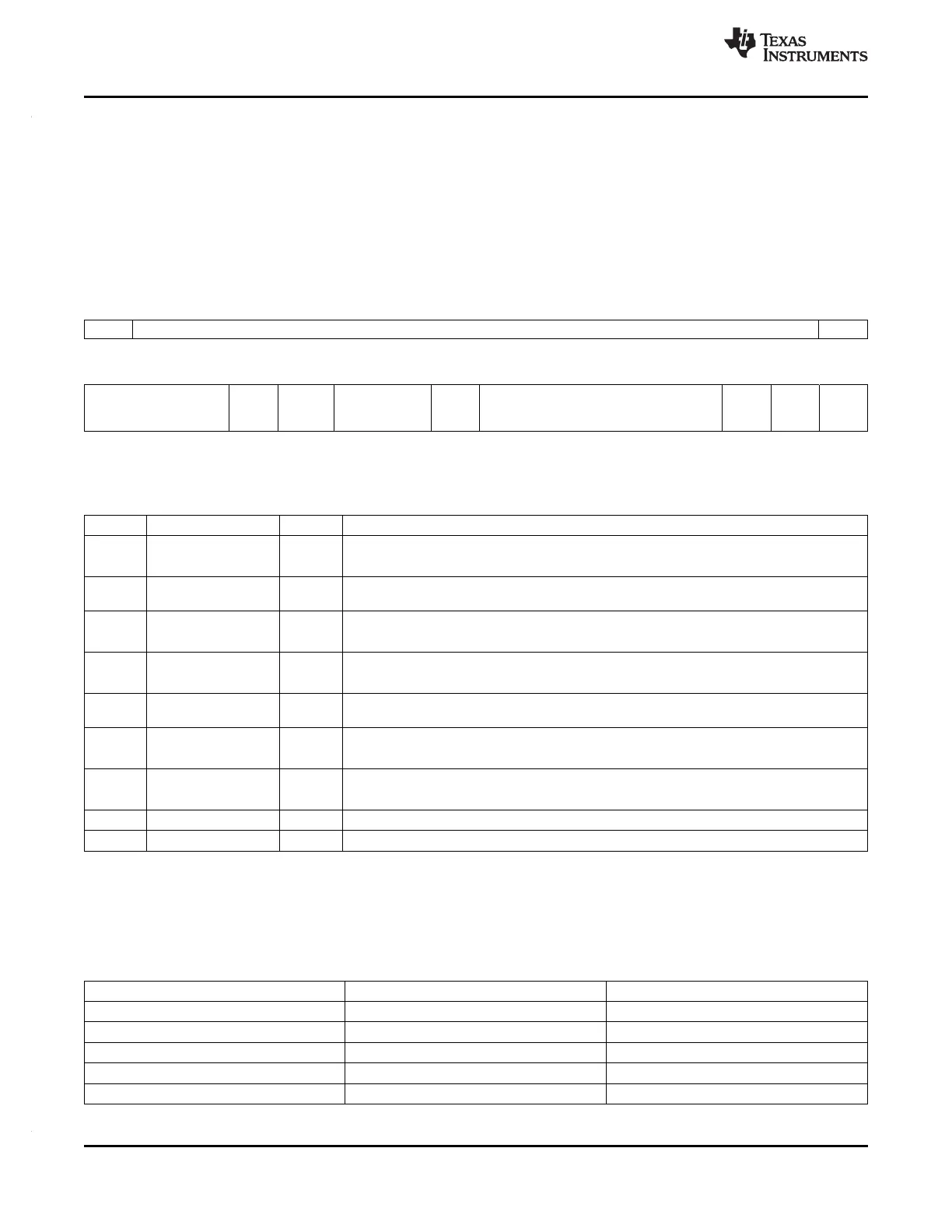
The device identification code register identifies several aspects of the device including the silicon version.
The details of the device identification code register are shown in Table 6-1. The device identification code
register value for this device is:
• Rev 0 = 0x8046AD05
Figure 6-2. Device ID Bit Allocation Register
31 30 29 28 27 26 25 24 23 22 21 20 19 18 17 16
CP-15 UNIQUE ID TECH
R-1 R-00000000100011 R-0
15 14 13 12 11 10 9 8 7 6 5 4 3 2 1 0
TECH I/O PERIPH FLASH ECC RAM VERSION 1 0 1
VOLT PARITY ECC
AGE
R-101 R-0 R-1 R-10 R-1 R-00000 R-1 R-0 R-1
LEGEND: R/W = Read/Write; R = Read only; -n = value after reset
Table 6-1. Device ID Bit Allocation Register Field Descriptions
Bit Field Value Description
31 CP15 Indicates the presence of coprocessor 15
1 CP15 present
30-17 UNIQUE ID 100011 Unique device identification number
This bitfield holds a unique number for a dedicated device configuration (die).
16-13 TECH Process technology on which the device is manufactured.
0101 F021
12 I/O VOLTAGE I/O voltage of the device.
0 I/O are 3.3v
11 PERIPHERAL 1 Peripheral Parity
PARITY Parity on peripheral memories
10-9 FLASH ECC Flash ECC
10 Program memory with ECC
8 RAM ECC Indicates if RAM memory ECC is present.
1 ECC implemented
7-3 REVISION Revision of the Device.
2-0 101 The platform family ID is always 0b101
6.3.2 Die Identification Registers
The four die ID registers at addresses 0xFFFFE1F0, 0xFFFFE1F4, 0xFFFFE1F8 and FFFFE1FC form a
128-bit dieid with the information as shown in Table Table 6-2.
Table 6-2. Die-ID Registers
Item # of Bits Bit Location
X Coord. on Wafer 8 7..0
Y Coord. on Wafer 8 15..8
Wafer # 6 21..16
Lot # 24 45..22
Reserved 82 127..46
166 Device and Documentation Support Copyright © 2012, Texas Instruments Incorporated
Submit Documentation Feedback