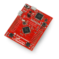
RM46L852
SPNS185 –SEPTEMBER 2012
www.ti.com
5.4 Multi-Buffered 12bit Analog-to-Digital Converter
The multibuffered A-to-D converter (MibADC) has a separate power bus for its analog circuitry that
enhances the A-to-D performance by preventing digital switching noise on the logic circuitry which could
be present on V
SS
and V
CC
from coupling into the A-to-D analog stage. All A-to-D specifications are given
with respect to AD
REFLO
unless otherwise noted.
Table 5-15. MibADC Overview
Description Value
Resolution 12 bits
Monotonic Assured
Output conversion code 00h to 3FFh [00 for V
AI
≤ AD
REFLO
; 3FFh for V
AI
≥ AD
REFHI
]
5.4.1 Features
• 12-bit resolution
• AD
REFHI
and AD
REFLO
pins (high and low reference voltages)
• Total Sample/Hold/Convert time: 600ns Minimum at 30MHz ADCLK
• One memory region per conversion group is available (event, group 1, group 2)
• Allocation of channels to conversion groups is completely programmable
• Supports flexible channel conversion order
• Memory regions are serviced either by interrupt or by DMA
• Programmable interrupt threshold counter is available for each group
• Programmable magnitude threshold interrupt for each group for any one channel
• Option to read either 8-bit, 10-bit or 12-bit values from memory regions
• Single or continuous conversion modes
• Embedded self-test
• Embedded calibration logic
• Enhanced power-down mode
– Optional feature to automatically power down ADC core when no conversion is in progress
• External event pin (ADxEVT) programmable as general-purpose I/O
5.4.2 Event Trigger Options
The ADC module supports 3 conversion groups: Event Group, Group1 and Group2. Each of these 3
groups can be configured to be hardware event-triggered. In that case, the application can select from
among 8 event sources to be the trigger for a group's conversions.
5.4.2.1 MIBADC1 Event Trigger Hookup
Table 5-16. MIBADC1 Event Trigger Hookup
Trigger Event Signal
Group Source
Select, G1SRC, PINMMR30[0] = 0 and PINMMR30[1] = 1
Event #
PINMMR30[0] = 1
G2SRC or
Control for Control for
(default)
Option A Option B
EVSRC
Option A Option B
000 1 AD1EVT AD1EVT — AD1EVT —
PINMMR30[8] = 0
001 2 N2HET1[8] N2HET2[5] PINMMR30[8] = 1 ePWM_B and
PINMMR30[9] = 1
010 3 N2HET1[10] N2HET1[27] — N2HET1[27] —
126 Peripheral Information and Electrical Specifications Copyright © 2012, Texas Instruments Incorporated
Submit Documentation Feedback
 Loading...
