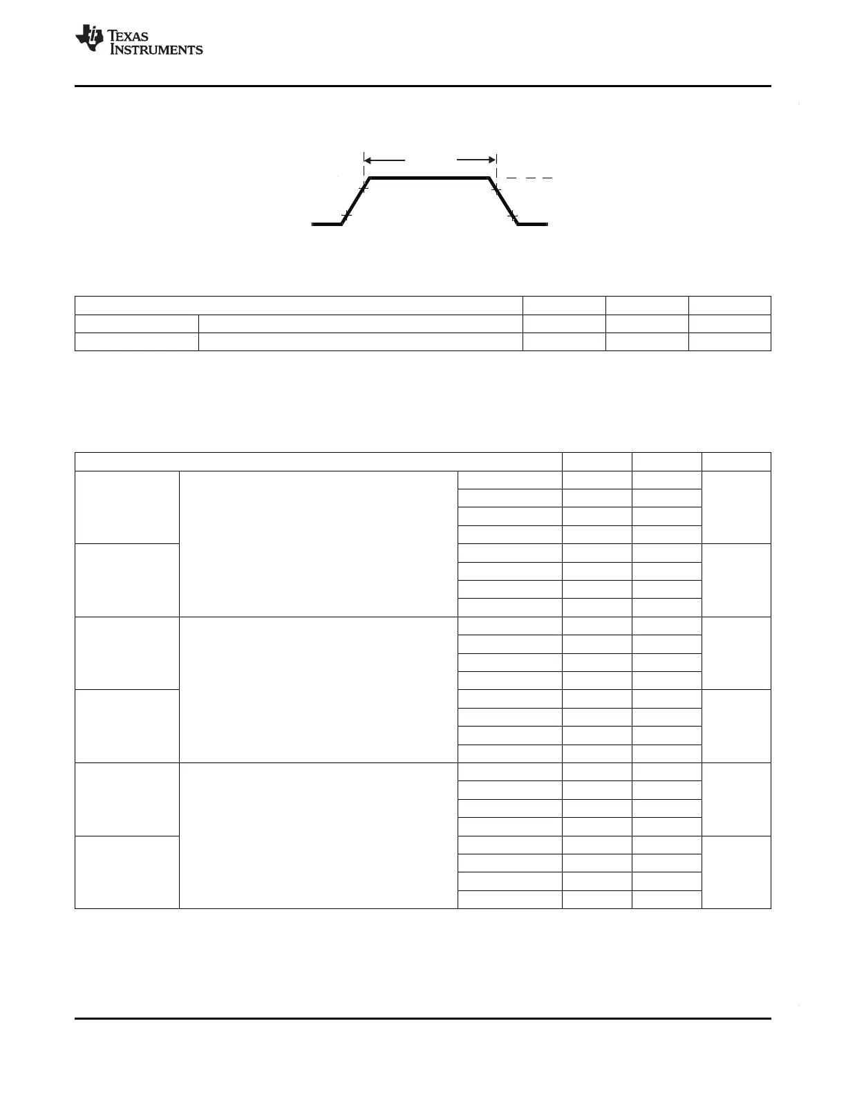
V
CCIO
V
IH
V
IH
V
IL
0
Input
t
pw
V
IL
RM46L852
www.ti.com
SPNS185 –SEPTEMBER 2012
3.8 Input Timings
Figure 3-2. TTL-Level Inputs
Table 3-3. Timing Requirements for Inputs
(1)
Parameter MIN MAX Unit
t
pw
Input minimum pulse width t
c(VCLK)
+ 10
(2)
ns
t
in_slew
Time for input signal to go from V
IL
to V
IH
or from V
IH
to V
IL
1 ns
(1) t
c(VCLK)
= peripheral VBUS clock cycle time = 1 / f
(VCLK)
(2) The timing shown above is only valid for pin used in general-purpose input mode.
3.9 Output Timings
Table 3-4. Switching Characteristics for Output Timings versus Load Capacitance (C
L
)
Parameter MIN MAX Unit
Rise time, t
r
8mA low EMI pins CL = 15 pF 2.5 ns
(see Table 3-2)
CL = 50 pF 4
CL = 100 pF 7.2
CL = 150 pF 12.5
Fall time, t
f
CL = 15 pF 2.5 ns
CL = 50 pF 4
CL = 100 pF 7.2
CL = 150 pF 12.5
Rise time, t
r
4mA low EMI pins CL = 15 pF 5.6 ns
(see Table 3-2)
CL = 50 pF 10.4
CL = 100 pF 16.8
CL = 150 pF 23.2
Fall time, t
f
CL = 15 pF 5.6 ns
CL= 50 pF 10.4
CL = 100 pF 16.8
CL = 150 pF 23.2
Rise time, t
r
2mA-z low EMI pins CL = 15 pF 8 ns
(see Table 3-2)
CL = 50 pF 15
CL = 100 pF 23
CL = 150 pF 33
Fall time, t
f
CL = 15 pF 8 ns
CL = 50 pF 15
CL = 100 pF 23
CL = 150 pF 33
Copyright © 2012, Texas Instruments Incorporated Device Operating Conditions 51
Submit Documentation Feedback