t
f
t
r
V
CCIO
V
OH
V
OH
V
OL
V
OL
0
Output
RM46L852
SPNS185 –SEPTEMBER 2012
www.ti.com
Table 3-4. Switching Characteristics for Output Timings versus Load Capacitance (C
L
) (continued)
Parameter MIN MAX Unit
Rise time, t
r
Selectable 8mA / 2mA-z 8mA mode CL = 15 pF 2 ns
pins
CL = 50 pF 4
(see Table 3-2)
CL = 100 pF 8
CL = 150 pF 11
Fall time, t
f
CL = 15 pF 2 ns
CL = 50 pF 4
CL = 100 pF 8
CL = 150 pF 11
Rise time, t
r
2mA-z mode CL = 15 pF 8 ns
CL = 50 pF 15
CL = 100 pF 23
CL = 150 pF 33
Fall time, t
f
CL = 15 pF 8 ns
CL = 50 pF 15
CL = 100 pF 23
CL = 150 pF 33
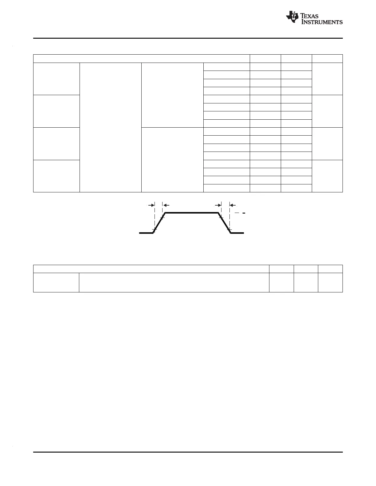
Figure 3-3. CMOS-Level Outputs
Table 3-5. Timing Requirements for Outputs
(1)
Parameter MIN MAX UNIT
t
d(parallel_out)
Delay between low to high, or high to low transition of general-purpose output signals 6 ns
that can be configured by an application in parallel, e.g. all signals in a GIOA port, or
all N2HET1 signals, etc.
(1) This specification does not account for any output buffer drive strength differences or any external capacitive loading differences. Check
Table 3-2 for output buffer drive strength information on each signal.
52 Device Operating Conditions Copyright © 2012, Texas Instruments Incorporated
Submit Documentation Feedback