RM46L852
www.ti.com
SPNS185 –SEPTEMBER 2012
3.10 Low-EMI Output Buffers
The low-EMI output buffer has been designed explicitly to address the issue of decoupling sources of
emissions from the pins which they drive. This is accomplished by adaptively controlling the impedance of
the output buffer, and is particularly effective with capacitive loads.
This is not the default mode of operation of the low-EMI output buffers and must be enabled by setting the
system module GPCR1 register for the desired module or signal, as shown in . The adaptive impedance
control circuit monitors the DC bias point of the output signal. The buffer internally generates two
reference levels, VREFLOW and VREFHIGH, which are set to approximately 10% and 90% of VCCIO,
respectively.
Once the output buffer has driven the output to a low level, if the output voltage is below VREFLOW, then
the output buffer’s impedance will increase to hi-Z. A high degree of decoupling between the internal
ground bus and the output pin will occur with capacitive loads, or any load in which no current is flowing,
e.g. the buffer is driving low on a resistive path to ground. Current loads on the buffer which attempt to pull
the output voltage above VREFLOW will be opposed by the buffer’s output impedance so as to maintain
the output voltage at or below VREFLOW.
Conversely, once the output buffer has driven the output to a high level, if the output voltage is above
VREFHIGH then the output buffer’s impedance will again increase to hi-Z. A high degree of decoupling
between internal power bus ad output pin will occur with capacitive loads or any loads in which no current
is flowing, e.g. buffer is driving high on a resistive path to VCCIO. Current loads on the buffer which
attempt to pull the output voltage below VREFHIGH will be opposed by the buffer’s output impedance so
as to maintain the output voltage at or above VREFHIGH.
The bandwidth of the control circuitry is relatively low, so that the output buffer in adaptive impedance
control mode cannot respond to high-frequency noise coupling into the buffer’s power buses. In this
manner, internal bus noise approaching 20% peak-to-peak of VCCIO can be rejected.
Unlike standard output buffers which clamp to the rails, an output buffer in impedance control mode will
allow a positive current load to pull the output voltage up to VCCIO + 0.6V without opposition. Also, a
negative current load will pull the output voltage down to VSSIO – 0.6V without opposition. This is not an
issue since the actual clamp current capability is always greater than the IOH / IOL specifications.
The low-EMI output buffers are automatically configured to be in the standard buffer mode when the
device enters a low-power mode.
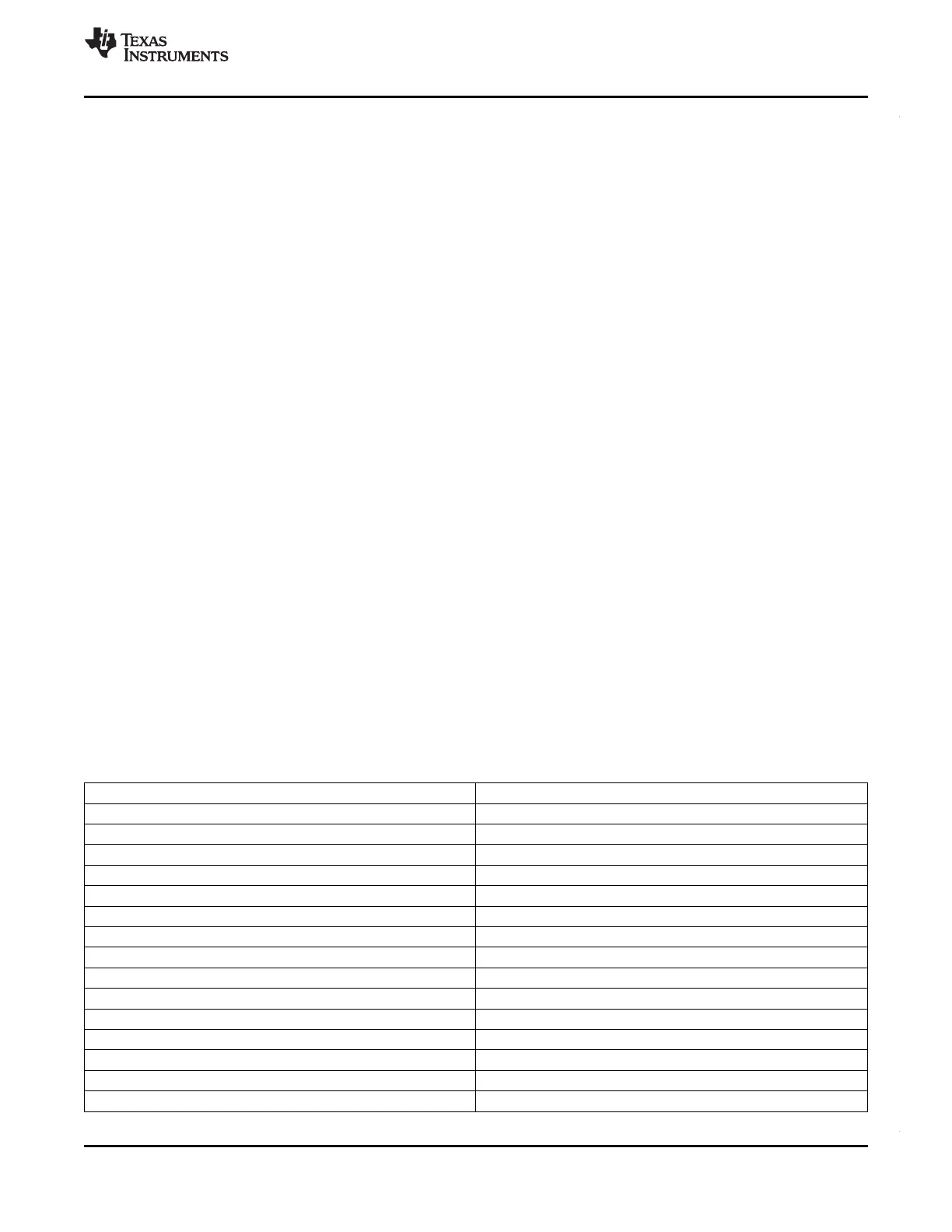
Table 3-6. Low-EMI Output Buffer Hookup
Module or Signal Name Control Register to Enable Low-EMI Mode
Module: MibSPI1 GPREG1.0
Module: SPI2 GPREG1.1
Module: MibSPI3 GPREG1.2
Reserved GPREG1.3
Module: MibSPI5 GPREG1.4
Reserved GPREG1.5
Module: EMIF GPREG1.6
Reserved GPREG1.7
Signal: TMS GPREG1.8
Signal: TDI GPREG1.9
Signal: TDO GPREG1.10
Signal: RTCK GPREG1.11
Signal: TEST GPREG1.12
Signal: nERROR GPREG1.13
Signal: AD1EVT GPREG1.14
Copyright © 2012, Texas Instruments Incorporated Device Operating Conditions 53
Submit Documentation Feedback