RM46L852
www.ti.com
SPNS185 –SEPTEMBER 2012
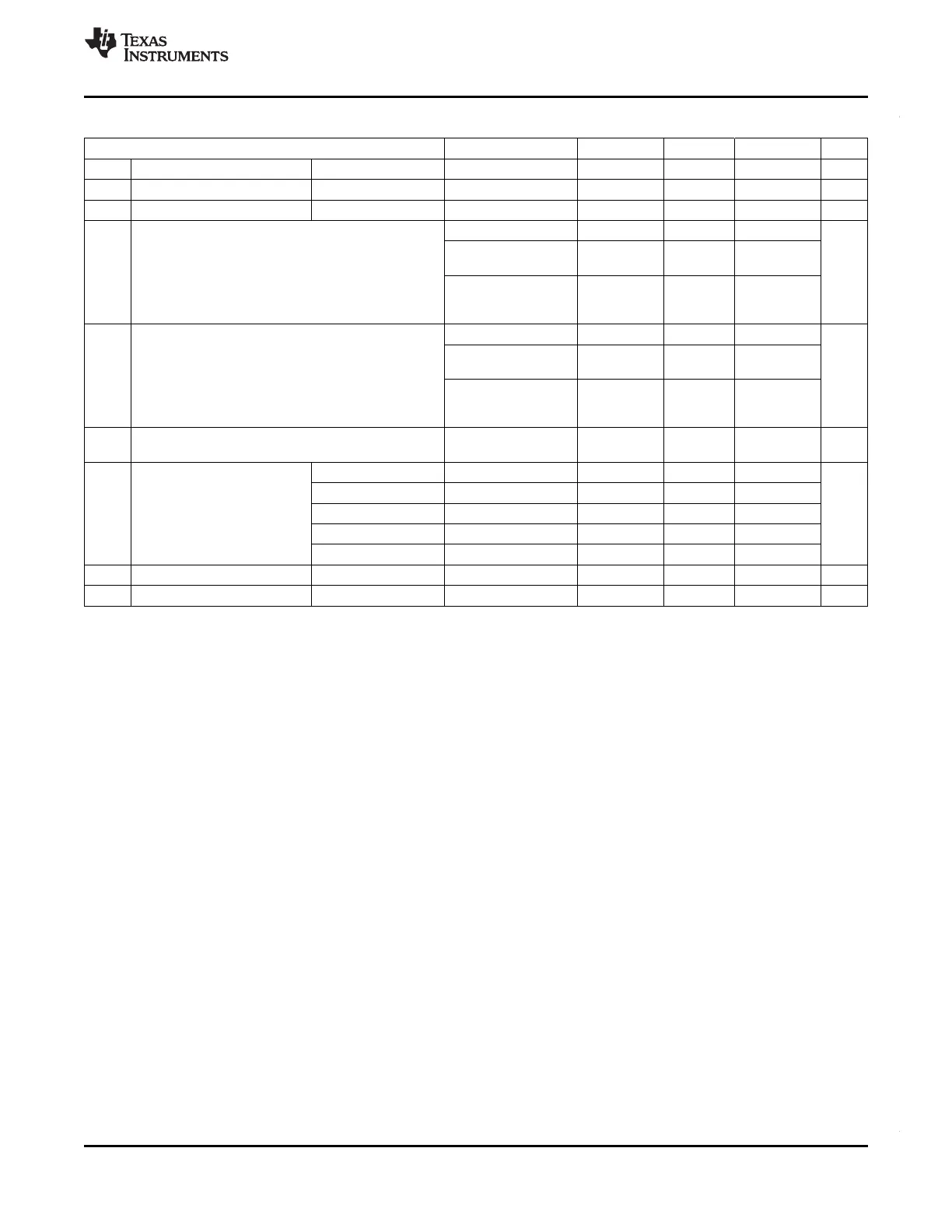
3.6 Input/Output Electrical Characteristics Over Recommended Operating Conditions
(1)
PARAMETER TEST CONDITIONS MIN TYP MAX UNIT
V
hys
Input hysteresis All inputs 180 mV
V
IL
Low-level input voltage All inputs -0.3 0.8 V
V
IH
High-level input voltage All inputs 2 V
CCIO
+ 0.3 V
I
OL
= I
OLmax
0.2 V
CCIO
I
OL
= 50 µA, standard 0.2
output mode
V
OL
Low-level output voltage V
I
OL
= 50 µA, low-EMI 0.2 V
CCIO
output mode (see
Section 3.10)
I
OH
= I
OHmax
0.8 V
CCIO
I
OH
= 50 µA, standard V
CCIO
-0.2
output mode
V
OH
High-level output voltage V
I
OH
= 50 µA, low-EMI 0.8 V
CCIO
output mode (see
Section 3.10)
V
I
< V
SSIO
- 0.3 or V
I
-2 2
I
IC
Input clamp current (I/O pins) mA
> V
CCIO
+ 0.3
I
IH
Pulldown 20µA V
I
= V
CCIO
5 40
I
IH
Pulldown 100µA V
I
= V
CCIO
40 195
I
I
Input current (I/O pins) I
IL
Pullup 20µA V
I
= V
SS
-40 -5 µA
I
IL
Pullup 100µA V
I
= V
SS
-195 -40
All other pins No pullup or pulldown -1 1
C
I
Input capacitance 2 pF
C
O
Output capacitance 3 pF
(1) Source currents (out of the device) are negative while sink currents (into the device) are positive.
Copyright © 2012, Texas Instruments Incorporated Device Operating Conditions 49
Submit Documentation Feedback