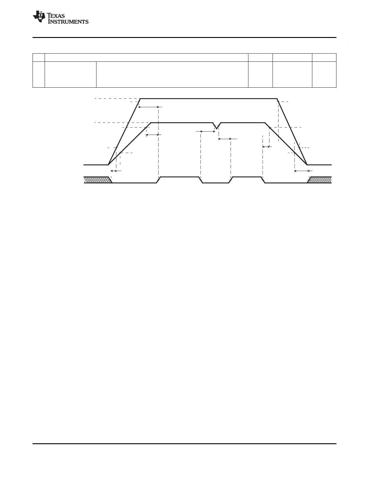
3.3 V
V
CCIOPORH
1.2 V
V
CCPORH
V
CCIOPORL
V (1.2 V)
V / V (3.3 V)
CC
CCIO CCP
nPORRST
8
6
6
7
7
93
V
CCPORL
V
IL(PORRST)
V / V
CCIO CCP
V
CC
V
CCPORL
V
IL(PORRST)
V
IL
V
IL
V
IL
V
CCIOPORH
V
CCPORH
V
CCIOPORL
NOTE: There is no timing dependency between the ramp of the VCCIO and the VCC supply voltage; this is just an exemplary drawing.
RM46L852
www.ti.com
SPNS185 –SEPTEMBER 2012
Table 4-4. Electrical Requirements for nPORRST (continued)
NO Parameter MIN MAX Unit
t
f(nPORRST)
500 2000 ns
Filter time nPORRST pin;
pulses less than MIN will be filtered out, pulses greater than MAX
will generate a reset.
Figure 4-1. nPORRST Timing Diagram
Copyright © 2012, Texas Instruments Incorporated System Information and Electrical Specifications 57
Submit Documentation Feedback