RM46L852
SPNS185 –SEPTEMBER 2012
www.ti.com
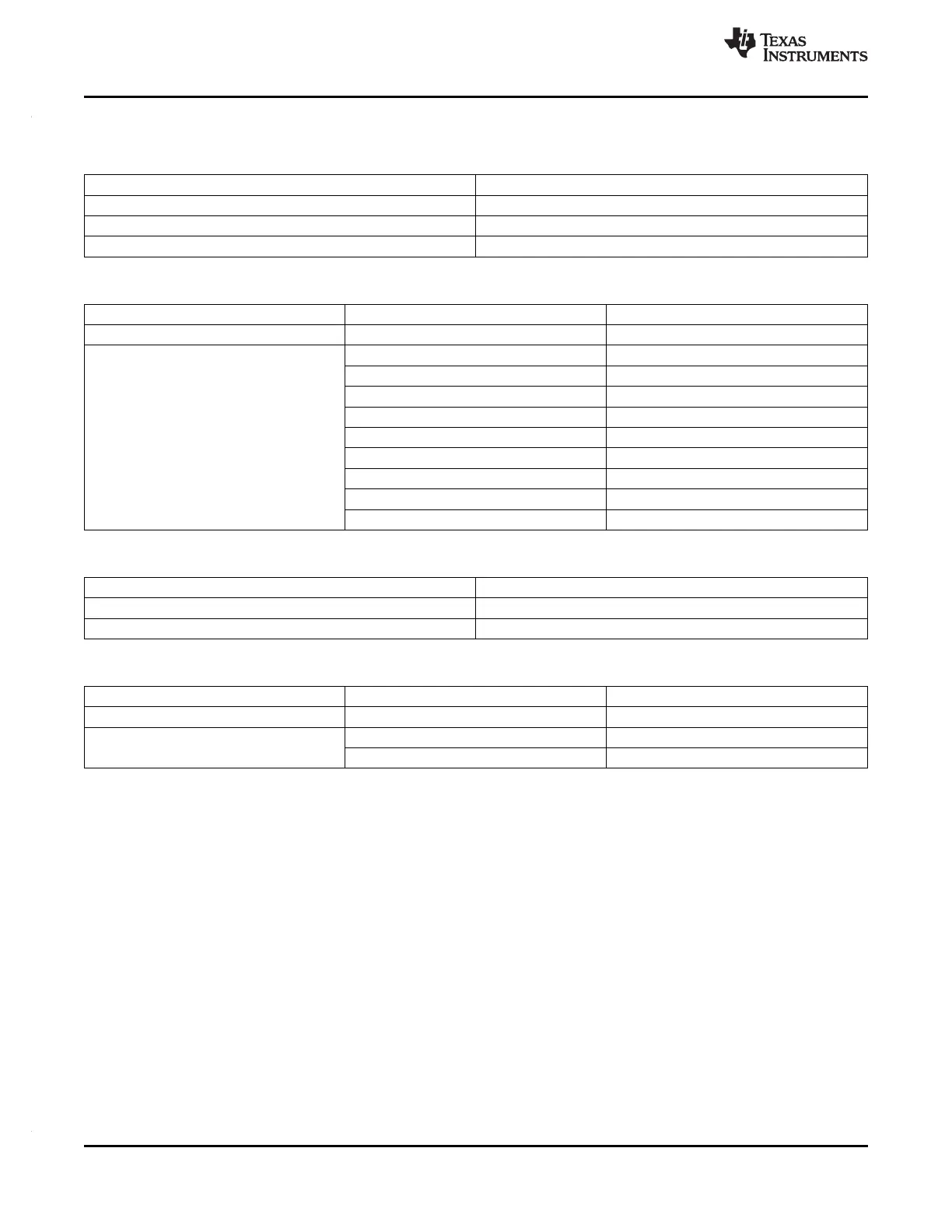
4.7.3.2 Mapping of DCC Clock Source Inputs
Table 4-16. DCC1 Counter 0 Clock Sources
CLOCK SOURCE [3:0] CLOCK NAME
others oscillator (OSCIN)
0x5 high frequency LPO
0xA test clock (TCK)
Table 4-17. DCC1 Counter 1 Clock Sources
KEY [3:0] CLOCK SOURCE [3:0] CLOCK NAME
others - N2HET1[31]
0x0 Main PLL free-running clock output
0x1 PLL #2 free-running clock output
0x2 low frequency LPO
0xA 0x3 high frequency LPO
0x4 reserved
0x5 EXTCLKIN1
0x6 EXTCLKIN2
0x7 reserved
0x8 - 0xF VCLK
Table 4-18. DCC2 Counter 0 Clock Sources
CLOCK SOURCE [3:0] CLOCK NAME
others oscillator (OSCIN)
0xA test clock (TCK)
Table 4-19. DCC2 Counter 1 Clock Sources
KEY [3:0] CLOCK SOURCE [3:0] CLOCK NAME
others - N2HET2[0]
0xA 00x0 - 0x7 Reserved
0x8 - 0xF VCLK
72 System Information and Electrical Specifications Copyright © 2012, Texas Instruments Incorporated
Submit Documentation Feedback