57
TMS320F28069
,
TMS320F28068
,
TMS320F28067
,
TMS320F28066
TMS320F28065, TMS320F28064, TMS320F28063, TMS320F28062
www.ti.com
SPRS698F –NOVEMBER 2010–REVISED MARCH 2016
Submit Documentation Feedback
Product Folder Links: TMS320F28069 TMS320F28068 TMS320F28067 TMS320F28066 TMS320F28065
TMS320F28064 TMS320F28063 TMS320F28062
Detailed DescriptionCopyright © 2010–2016, Texas Instruments Incorporated
Peripheral Frame 1 and Peripheral Frame 2 are grouped together to enable these blocks to be write/read
peripheral block protected. The protected mode makes sure that all accesses to these blocks happen as
written. Because of the pipeline, a write immediately followed by a read to different memory locations, will
appear in reverse order on the memory bus of the CPU. This can cause problems in certain peripheral
applications where the user expected the write to occur first (as written). The CPU supports a block
protection mode where a region of memory can be protected so that operations occur as written (the
penalty is extra cycles are added to align the operations). This mode is programmable and by default, it
protects the selected zones.
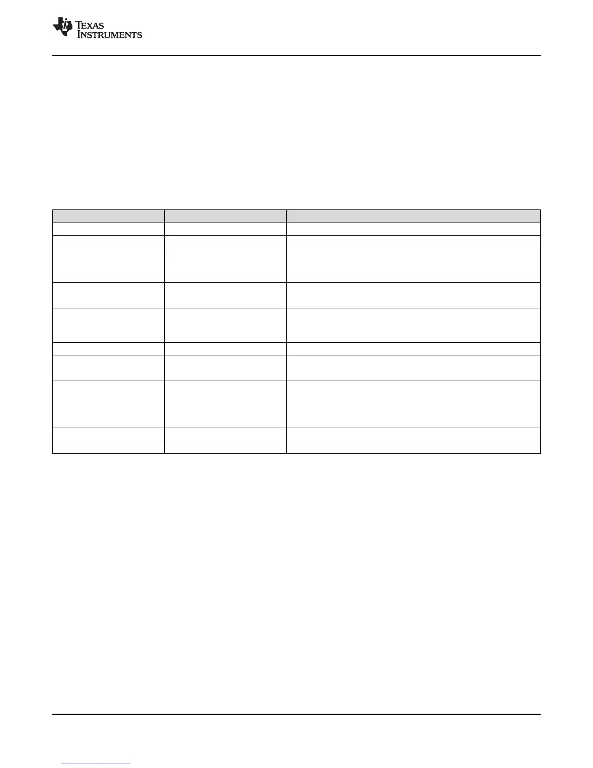
The wait-states for the various spaces in the memory map area are listed in Table 6-5.
Table 6-5. Wait-States
AREA WAIT-STATES (CPU) COMMENTS
M0 and M1 SARAMs 0-wait Fixed
Peripheral Frame 0 0-wait
Peripheral Frame 1 0-wait (writes) Cycles can be extended by peripheral-generated ready.
2-wait (reads) Back-to-back write operations to Peripheral Frame 1 registers will incur
a 1-cycle stall (1-cycle delay).
Peripheral Frame 2 0-wait (writes) Fixed. Cycles cannot be extended by the peripheral.
2-wait (reads)
Peripheral Frame 3 0-wait (writes) Assumes no conflict between CPU and CLA/DMA cycles. The wait
states can be extended by peripheral-generated ready.
2-wait (reads)
L0–L8 SARAM 0-wait data and program Assumes no CPU conflicts
OTP Programmable Programmed through the Flash registers.
1-wait minimum 1-wait is minimum number of wait states allowed.
FLASH Programmable Programmed through the Flash registers.
0-wait Paged min
1-wait Random min
Random ≥ Paged
FLASH Password 16-wait fixed Wait states of password locations are fixed.
Boot-ROM 0-wait