Do you have a question about the Toshiba T1200 and is the answer not in the manual?
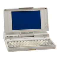
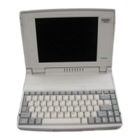
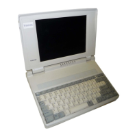
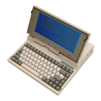
Introduction to the Toshiba T1200 portable personal computer and its features.
Details on the components composing the System PCB, including CPU, memory, and controllers.
Specifications and description of the 3.5-inch floppy disk drive used in the T1200.
Specifications and description of the 3.5-inch hard disk drive used in the T1200.
Description and specifications of the Hard Disk Control PCB (HDC).
Description of the T1200 keyboard, including key count and connectivity.
Specifications and description of the Liquid Crystal Display (LCD) unit.
Description of the Power Supply PCB, its functions, and output ratings.
Description and specifications of the built-in modem for communication.
Overview of procedures for isolating defective FRUs (Field Replaceable Units).
A flowchart guide for determining which FRU is defective.
Step-by-step procedures to diagnose issues with the Power Supply PCB.
Procedure to check the system's battery status.
Procedure to check the Power Supply indicator lights and their meaning.
Procedure to verify the proper connection of power supply and system PCB connectors.
Procedure to check the output voltages of the power supply PCB connectors.
Procedure for replacing the Power Supply PCB.
Step-by-step procedures to diagnose issues with the System PCB.
Procedure to check for specific system messages indicating PCB status.
Procedure to check system status via Printer Port LED.
Procedure to confirm the correct status of system PCB jumper straps.
Procedure to execute diagnostic test programs for the system.
Procedure for replacing the System PCB.
Step-by-step procedures to diagnose issues with the Floppy Disk Drive (FDD).
Check for correct loading of diagnostic programs into the FDD.
Check for specific messages during FDD diagnostic loading.
Procedure to clean the FDD heads using a cleaning disk.
Procedure to execute floppy disk drive tests and interpret error statuses.
Procedure to verify the secure connection of the FDD cable to the system PCB.
Procedure for connecting a new FDD and testing system operation.
Step-by-step procedures to diagnose issues with the Hard Disk Drive (HDD).
Check the HDD indicator status for diagnostics.
Procedure for executing hard disk formatting.
Procedure to execute hard disk drive tests and interpret error codes.
Procedure to verify the connection of HDD, HDC, and system PCB.
Procedure to confirm the correct status of jumper straps on HDC and system PCB.
Procedure for connecting a new HDC and testing system operation.
Procedure for connecting a new HDD and testing system operation.
Step-by-step procedures to diagnose issues with the keyboard.
Procedure to check keyboard input by typing characters on screen.
Procedure to execute keyboard tests and check for errors.
Procedure to verify the secure connection of the keyboard cable to the system PCB.
Procedure for connecting a new keyboard and testing system operation.
Step-by-step procedures to diagnose issues with the Liquid Crystal Display (LCD).
Procedure to check for the 'MEMORY TEST XXXKB' message on screen.
Procedure to adjust and check the LCD contrast knob functionality.
Procedure to execute display tests and check for system PCB issues.
Procedure to verify the LCD cable connection to the system PCB connector.
Procedure to verify the LCD cable connection to the LCD module.
Procedure for connecting a new LCD cable.
Procedure for connecting a new LCD module.
Overview of test and diagnostic programs for checking T1200 hardware modules.
Instructions on how to run the diagnostic programs and interpret results.
A table listing subtest names for the diagnostic test program.
Detailed descriptions of System Test subtests (ROM checksum, HDD off-SW).
Detailed descriptions of Memory Test subtests (RAM constant data, refresh, etc.).
Detailed descriptions of Keyboard Test subtests (key display, scan codes).
Detailed descriptions of Display Test subtests (VRAM, character attributes, graphics).
Detailed descriptions of Floppy Disk Test subtests (sequential read/write, random access).
Detailed descriptions of Printer Test subtests (ripple pattern, function, wrap around).
Detailed descriptions of Async Test subtests (wrap around, point-to-point).
Detailed descriptions of Hard Disk Test subtests (sequential read, address uniqueness).
Detailed descriptions of Real Timer Test subtests (real time input, real time carry).
Description of the NDP Test subtest.
Description of Expansion Unit Test subtests (box wrap around, video ram).
A table listing error codes and their corresponding status names for various devices.
Description and operations for physical formatting of the hard disk.
Description and operations for cleaning the FDD head.
Description of the Log Utilities program for logging error information.
Description and operations for the Running Test program.
Description and operations for FDD utilities: format, copy, and dump.
Description and operations for displaying system configuration.
Wiring diagrams for printer and RS232C wrap around connectors.
General information and precautions for replacing FRUs (Field Replaceable Units).
Detailed steps for removing the top cover assembly.
Steps for disconnecting the top cover assembly, including the LCD cable.
Detailed steps for removing and replacing the keyboard unit.
Detailed steps for removing/replacing memory card, RTC battery, and speaker.
Detailed steps for removing/replacing keyboard bridge and indicator PCB.
Detailed steps for removing and replacing the built-in modem.
Detailed steps for removing and replacing the Power Supply PCB.
Detailed steps for removing and replacing the FDD base.
Detailed steps for removing and replacing the Floppy Disk Drive (FDD).
Detailed steps for removing and replacing the Hard Disk Control PCB.
Detailed steps for removing and replacing the Hard Disk Drive (HDD).
Detailed steps for removing and replacing the System PCB.
Detailed steps for removing and replacing the LCD Mask.
Detailed steps for removing and replacing the LCD Module.
Detailed steps for removing the LCD Cover Subassembly.
Detailed steps for replacing the LCD Cover Subassembly.
Overview of the system unit's internal components and external interfaces.
Identification of internal components within the system unit.
Identification of connectors and controls on the rear panel of the system unit.
Identification of controls on the left side of the system unit.
Detailed layout of connectors and ICs on the System PCB.
List and description of connectors on the System PCB.
Identification of Integrated Circuits (ICs) on the System PCB.
Detailed pin descriptions for various system connectors.
Pin descriptions for the printer connector.
Pin descriptions for the external FDD connector.
Pin descriptions for the RGB connector.
Pin descriptions for the COMMS connector.
Pin descriptions for the COMP connector.
Pin descriptions for the Key pad connector.
Pin descriptions for the expansion bus connector.
Illustrations of keyboard layouts for different language versions.
Illustration of the USA keyboard layout.
Illustration of the England keyboard layout.
Illustration of the German keyboard layout.
Illustration of the France keyboard layout.
Illustration of the Spain keyboard layout.
Illustration of the Italy keyboard layout.
Illustration of the Scandinavia keyboard layout.
Illustration of the Switzerland keyboard layout.
Diagram showing keycap numbering.
A table showing display codes for characters.
General description of the Bus Controller Gate Array chip.
Block diagram of the Bus Controller Gate Array.
Detailed pin descriptions for the Bus Controller Gate Array.
Detailed descriptions of each functional block within the gate array.
Description of the clock generator function.
Description of the command decoder function.
Description of the bus controller function.
Description of the 8-16 bit conversion controller function.
Description of the wait controller function.
Description of the DMA bus controller function.
Description of the DMA Page register function.
Description of the RAM/ROM select controller function.
Description of the keyboard data controller function.
Description of circuitry compatible with the Intel 8255 chip.
Description of the I/O decoder circuit.
Description of the back-up port function.
General description of the I/O driver gate array.
Block diagram of the PRT/FDD Gate Array.
Detailed pin descriptions for the PRT/FDD Gate Array.
Functions of the FDD Controller, including register descriptions.
Description of the Digital Input Register for the FDD Controller.
Description of the Digital Output Register for the FDD Controller.
Description of the X-Rate register for the FDD Controller.
Functions of the Printer Controller, including register descriptions.
Description of the Data Register output for the Printer Controller.
Description of the Data Register input for the Printer Controller.
Description of the Status Register for the Printer Controller.
Description of the Control Register Output for the Printer Controller.
Description of the Printer mode register for the Printer Controller.
General description of the Bus Driver Gate Array.
Description of the functions performed by the Bus Driver Gate Array.
Block diagram of the Bus Driver Gate Array.
Detailed pin descriptions for the Bus Driver Gate Array.
Description of the I/O Decoder circuit.
Description of the Back-Up Port function.
General description of the Display Controller Gate Array.
Description of the Display Controller Subsystem (DCS).
Detailed pin descriptions for the Display Controller.
Functions of the Display Controller Subsystem (DCS).
Description of the video signals used for LCD and CRT displays.
Description of signals that select display modes (font, flat display).
Description of clock input signals for CRT and plasma displays.
Description of other signals like GA Off and LCD Duty select.
Overview of various signal groups within the DCS.
General description of the Expanded Memory Controller Gate Array.
Memory assignment map for the Expanded Memory Unit.
Detailed pin descriptions for the EMC Gate Array.
Description of the configuration port and registers for the EM unit.
Description of the Index Register (PORT 0EEH) for write operations.
Description of EM Configuration Register 0 (Index 50/60).
Description of EM Configuration Register 1 (Index 51/61).
| RAM | 1 MB |
|---|---|
| Graphics | CGA |
| Storage | 20 MB HDD |
| Operating System | MS-DOS |
| Ports | Serial, Parallel, External Floppy Disk Drive |
| Battery | NiCad |