VCU118 Board User Guide 96
UG1224 (v1.0) December 15, 2016
www.xilinx.com
Chapter 3: Board Component Descriptions
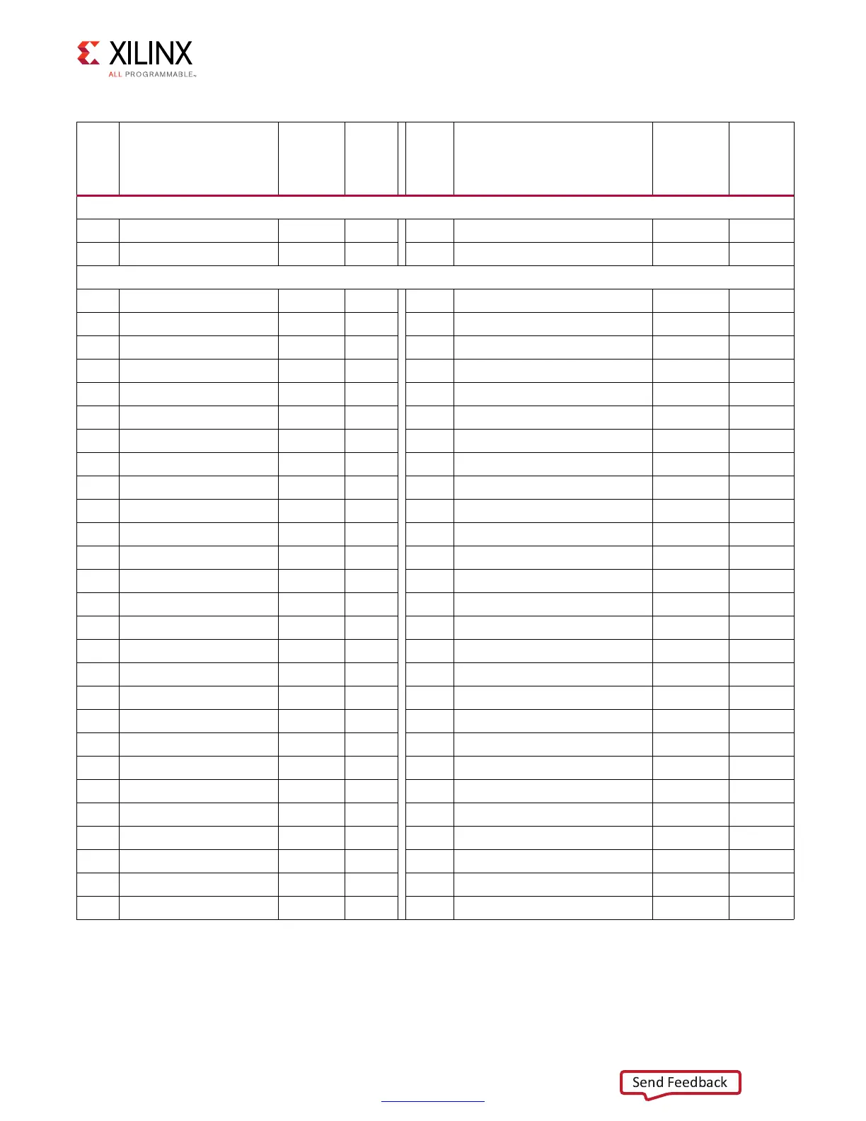
J2 Sections E/F have only the connections shown
E 39 V AD J _1 V 8_ F PG A
F1 FMC_HPC1_PG_M2C (6) LVCMOS18 BA7
F40 VADJ_1V8_FPGA
J2 Sections G/H Connections to FPGA U1
G2 FMC_HPC1_CLK1_M2C_P LVDS AV14
H1 FMC_HPC1_VREF_A_M2C LVCMOS18
G3 FMC_HPC1_CLK1_M2C_N LVDS AV13 H2 FMC_HPC1_PRSNT_M2C LVCMOS18 BB7
G6 FMC_HPC1_LA00_CC_P LVDS AY9 H4 FMC_HPC1_CLK0_M2C_P LVDS BC9
G7 FMC_HPC1_LA00_CC_N LVDS BA9 H5 FMC_HPC1_CLK0_M2C_N LVDS BC8
G9 FMC_HPC1_LA03_P LVDS BD12 H7 FMC_HPC1_LA02_P LVDS BC11
G10 FMC_HPC1_LA03_N LVDS BE12 H8 FMC_HPC1_LA02_N LVDS BD11
G12 FMC_HPC1_LA08_P LVDS BE15 H10 FMC_HPC1_LA04_P LVDS BF12
G13 FMC_HPC1_LA08_N LVDS BF15 H11 FMC_HPC1_LA04_N LVDS BF11
G15 FMC_HPC1_LA12_P LVDS BC14 H13 FMC_HPC1_LA07_P LVDS BC15
G16 FMC_HPC1_LA12_N LVDS BC13 H14 FMC_HPC1_LA07_N LVDS BD15
G18 FMC_HPC1_LA16_P LVDS AV9 H16 FMC_HPC1_LA11_P LVDS BA16
G19 FMC_HPC1_LA16_N LVDS AV8 H17 FMC_HPC1_LA11_N LVDS BA15
G21 FMC_HPC1_LA20_P LVDS AW11 H19 FMC_HPC1_LA15_P LVDS BB16
G22 FMC_HPC1_LA20_N LVDS AY10 H20 FMC_HPC1_LA15_N LVDS BC16
G24 FMC_HPC1_LA22_P LVDS AW13 H22 FMC_HPC1_LA19_P LVDS AW12
G25 FMC_HPC1_LA22_N LVDS AY13 H23 FMC_HPC1_LA19_N LVDS AY12
G27 FMC_HPC1_LA25_P LVDS AT12 H25 FMC_HPC1_LA21_P LVDS AU11
G28 FMC_HPC1_LA25_N LVDS AU12 H26 FMC_HPC1_LA21_N LVDS AV11
G30 FMC_HPC1_LA29_P LVDS AN15 H28 FMC_HPC1_LA24_P LVDS AP13
G31 FMC_HPC1_LA29_N LVDS AP15 H29 FMC_HPC1_LA24_N LVDS AR13
G33 FMC_HPC1_LA31_P LVDS AM13 H31 FMC_HPC1_LA28_P LVDS AV10
G34 FMC_HPC1_LA31_N LVDS AM12 H32 FMC_HPC1_LA28_N LVDS AW10
G36 FMC_HPC1_LA33_P LVDS AK14 H34 FMC_HPC1_LA30_P LVDS AK12
G37 FMC_HPC1_LA33_N LVDS AK13 H35 FMC_HPC1_LA30_N LVDS AL12
G39 VAD J_1 V8_FP GA H37 FMC _HPC1 _LA32 _P LVDS AJ 13
H38 FMC_HPC1_LA32_N LVDS AJ12
H40 VADJ_1V8_FPGA
Table 3-31: J2 VITA 57.1 FMC HPC1 Connections (Cont’d)
J2
FMC
HPC1
Pin
Schematic Net Name
I/O
Standard
FPGA
(U1)
Pin
J2
FMC
HPC1
Pin
Schematic Net Name
I/O
Standard
FPGA
(U1) Pin