VCU118 Board User Guide 88
UG1224 (v1.0) December 15, 2016
www.xilinx.com
Chapter 3: Board Component Descriptions
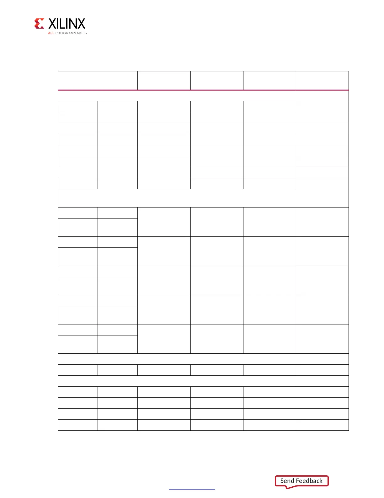
Table 3-29 lists the GPIO connections to FPGA U1.
Table 3-29: VCU118 GPIO Connections to FPGA U1
FPGA (U1) Pin
Schematic Net
Name
FPGA (U1)
Direction
I/O Standard Device
GPIO LEDs (Active-High) GPIO_LED signals are wired to FET LED drivers
BANK 40 AT32 GPIO_LED_0 Output LVCMOS12 DS7
BANK 40 AV34 GPIO_LED_1 Output LVCMOS12 DS6
BANK 40 AY30 GPIO_LED_2 Output LVCMOS12 DS8
BANK 40 BB32 GPIO_LED_3 Output LVCMOS12 DS9
BANK 40 BF32 GPIO_LED_4 Output LVCMOS12 DS10
BANK 42 AU37 GPIO_LED_5 Output LVCMOS12 DS12
BANK 42 AV36 GPIO_LED_6 Output LVCMOS12 DS13
BANK 42 BA37 GPIO_LED_7 Output LVCMOS12 DS18
Directional pushbuttons (Active-High) are wired in parallel to FPGA BANK 64 and system controller U111
Bank 501
BANK 64 BB24
GPIO_SW_N Input LVCMOS18 SW10.3
BANK 501
U111
A13
BANK 64 BE23
GPIO_SW_E Input LVCMOS18 SW9.3
BANK 501
U111
B14
BANK 64 BF22
GPIO_SW_W Input LVCMOS18 SW6.3
BANK 501
U111
D14
BANK 64 BE22
GPIO_SW_S Input LVCMOS18 SW17.3
BANK 501
U111
C14
BANK 64 BD23
GPIO_SW_C Input LVCMOS18 SW7.3
BANK 501
U111
B12
CPU reset pushbutton (active-high)
BANK 73 L19 CPU_RESET Input LVCMOS12 SW5.3
4-Pole DIP SW (active-high)
BANK 73 B17 GPIO_DIP_SW0 Input LVCMOS12 SW12.4
BANK 73 G16 GPIO_DIP_SW1 Input LVCMOS12 SW12.3
BANK 73 J16 GPIO_DIP_SW2 Input LVCMOS12 SW12.2
BANK 72 D21 GPIO_DIP_SW3 Input LVCMOS12 SW12.1