VCU118 Board User Guide 11
UG1224 (v1.0) December 15, 2016
www.xilinx.com
Chapter 2: Board Setup and Configuration
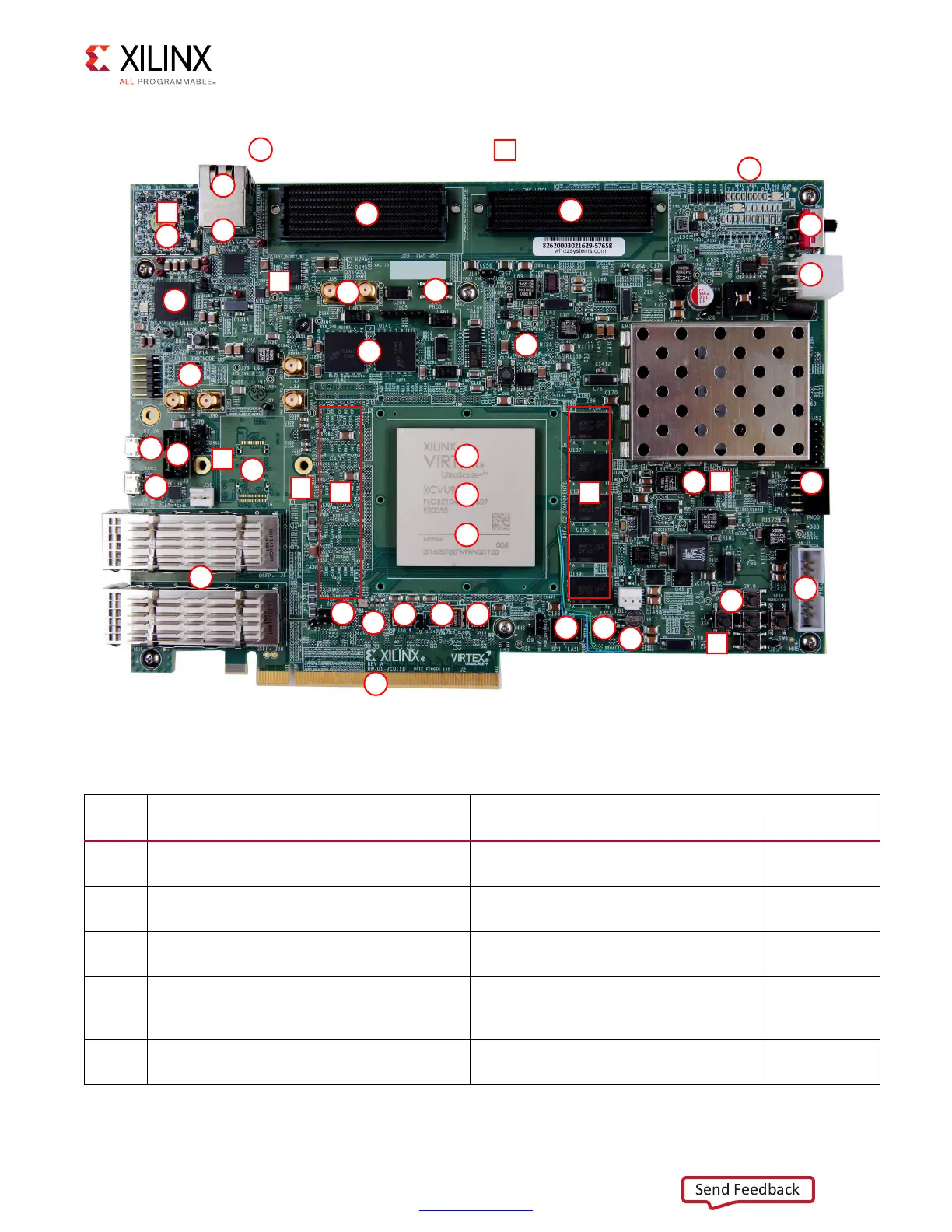
X-Ref Target - Figure 2-1
Figure 2-1: VCU118 Evaluation Board Components
Round callout references a component
on the front side of the board
Square callout references a component
on the backside side of the board
9
7
20
19
36
28
38
8
21
14
18
26
17
4
C1
40
5
33
34
22
15
27
23
24
30
39
29
37
25
11
31
31
4
C2
16
13 12 35
6 10
11
2
1
3
00
00
41
X18022-102616
Table 2-1: VCU118 Board Component Descriptions
Callout Feature Notes
Schematic
Page Number
1
Virtex UltraScale+ XCVU9P-L2FLGA2104
Device, (with fan-sink on soldered FPGA)
XCVU9P-L2FLGA2104E
Cofan 30-5530-03
2
GTY transceivers, Right Side Quads (six
quads)
Embedded within FPGA U1 14-15
3
GTY transceivers, Left Side Quads (seven
quads)
Embedded within FPGA U1 16-17
4
DDR4 Component Memory, two 80-bit DDR4
component memory I/F, C1 (U60-U64)
(bottom) and C2 (U135-U139) (top)
C1: 5 x Micron MT40A256M16GE-075E,
C2: 5 x Micron MT40A256M16GE-075E
25-27,
28-30
5
RLD3 Component Memory, RLD3 72-bit
component memory I/F C3 (U141-U142)
Micron MT44K32M36RB-083F 31-32