VCU118 Board User Guide 73
UG1224 (v1.0) December 15, 2016
www.xilinx.com
Chapter 3: Board Component Descriptions
The connections between the 28 Gb/s QSFP+ module connector U145 and the FPGA are
listed in Table 3-22.
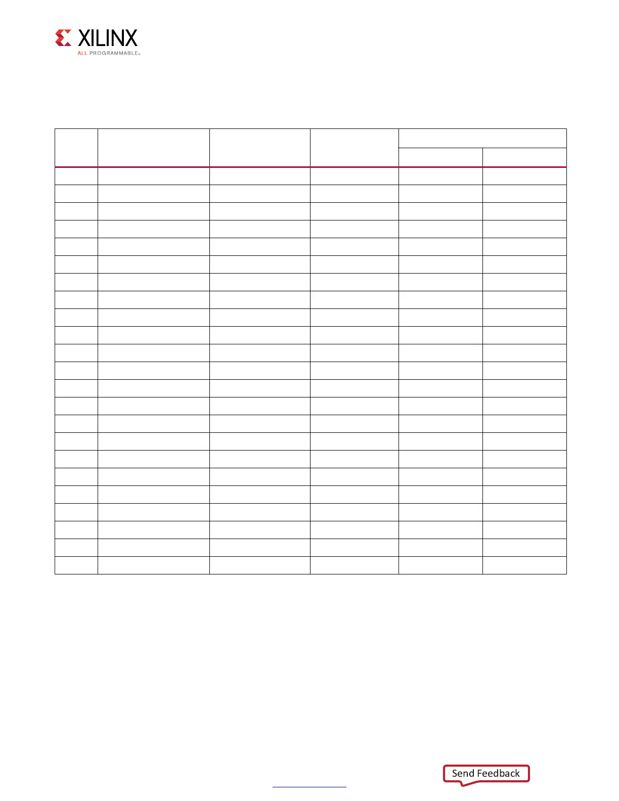
Table 3-22: VCU118 Board FPGA U1 to QSFP+ Module QSFP1 U145 Connections
FPGA
(U1) Pin
FPGA (U1) Pin Name
Schematic Net
Name
FPGA (U1)
Direction
QSFP1 U145
Pin Num Pin Name
V7 MGTYTXP0_231 QSFP1_TX1_P Output 36 TX1P
V6 MGTYTXN0_231 QSFP1_TX1_N Output 37 TX1N
Y2 MGTYRXP0_231 QSFP1_RX1_P Input 17 RX1P
Y1 MGTYRXN0_231 QSFP1_RX1_N Input 18 RX1N
T7 MGTYTXP1_231 QSFP1_TX2_P Output 3 TX2P
T6 MGTYTXN1_231 QSFP1_TX2_N Output 2 TX2N
W4 MGTYRXP1_231 QSFP1_RX2_P Input 22 RX2P
W3 MGTYRXN1_231 QSFP1_RX2_N Input 21 RX2N
P7 MGTYTXP2_231 QSFP1_TX3_P Output 33 TX3P
P6 MGTYTXN2_231 QSFP1_TX3_N Output 34 TX3N
V2 MGTYRXP2_231 QSFP1_RX3_P Input 14 RX3P
V1 MGTYRXN2_231 QSFP1_RX3_N Input 15 RX3N
M7 MGTYTXP3_231 QSFP1_TX4_P Output 6 TX4P
M6 MGTYTXN3_231 QSFP1_TX4_N Output 5 TX4N
U4 MGTYRXP3_231 QSFP1_RX4_P Input 25 RX4P
U3 MGTYRXN3_231 QSFP1_RX4_N Input 24 RX4N
U28.9 SC2 QSFP1_IIC_SCL
(1)
Output 11 SCL
U28.8 SD2 QSFP1_IIC_SDA
(1)
BiDir 12 SDA
AM21 IO_L23N_T3U_N9_64 QSFP1_MODSELL
(2)
Output 8 MODSELL
BA22 IO_L10N_T1U_N7_64 QSFP1_RESETL
(2)
Output 9 RESETL
AL21 IO_L23P_T3U_N8_64 QSFP1_MODPRSL
(2)
Output 27 MODPRSL
AP21 IO_L21N_T3L_N5_64 QSFP1_INTL
(2)
Input 28 INTL
AN21 IO_L21P_T3L_N4_64 QSFP1_LPMODE
(2)
Output 31 LPMODE
Notes:
1. The QSFP+ connectors U145 I
2
C SCL/SDA are connected via I
2
C switch U28 to the IIC_MAIN_SCL/SDA bus. See I2C Bus,
Topology, and Switches.
2. The QSFP+ connector U145 QSFP1 control signals are level-shifted by U17.