VCU118 Board User Guide 93
UG1224 (v1.0) December 15, 2016
www.xilinx.com
Chapter 3: Board Component Descriptions
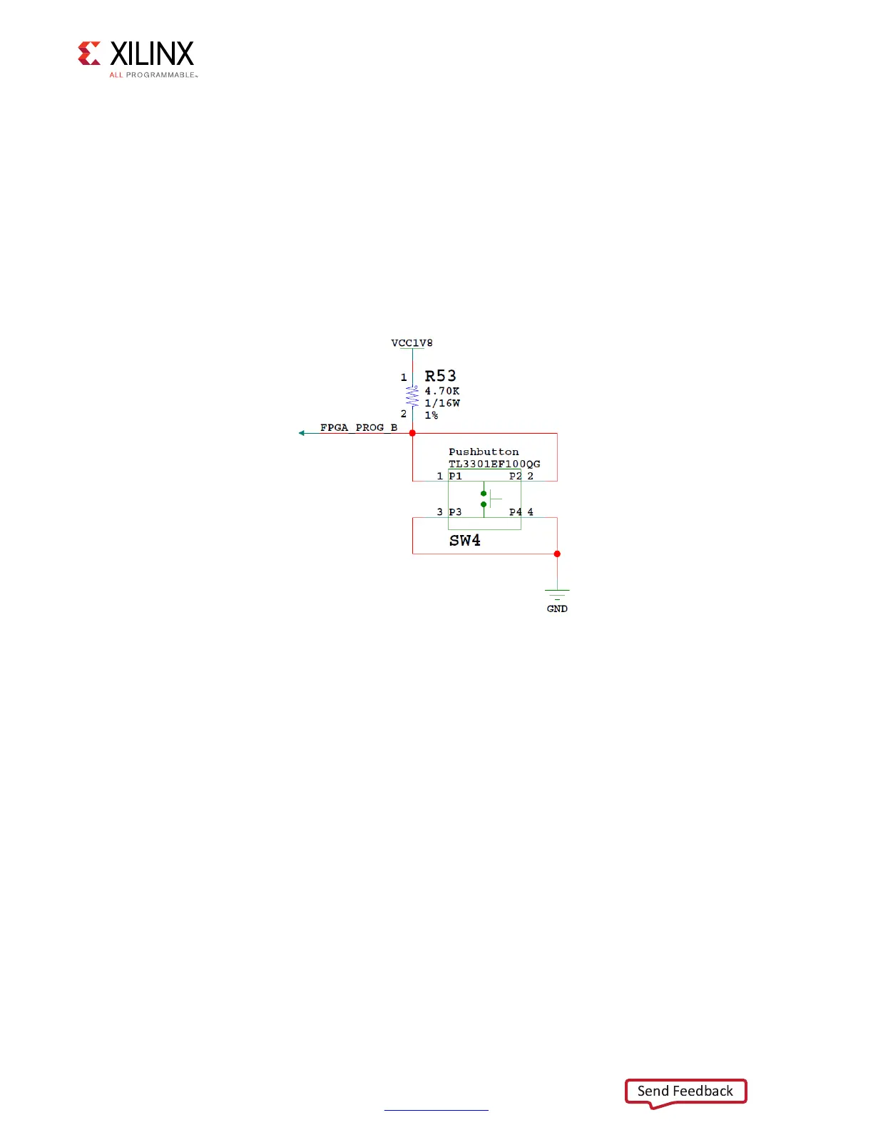
Program_B Pushbutton Switch
[Figure 2-1, callout 27]
Switch SW4 grounds the XCVU9P FPGA U1 PROGRAM_B pin when pressed. This action
clears the FPGA configuration. The FPGA_PROG_B signal is connected to XCVU9P FPGA U1
pin AH11. See UltraScale Architecture Configuration User Guide (UG570) [Ref 2] for further
configuration details.
Figure 3-26 shows SW4.
FPGA Mezzanine Card Interface
[Figure 2-1, callouts 33, 34]
The VCU118 evaluation board supports the VITA 57.1 FPGA mezzanine card (FMC)
specification by providing a subset implementation of the high pin count connector at J2
(HPC1). HPC connectors use a 10 x 40 form factor, populated with 400 pins. The connector
is keyed so that a mezzanine card, when installed on the VCU118 evaluation board, faces
away from the board.
In addition, the VCU118 evaluation board supports the VITA 57.4 FPGA mezzanine card plus
(FMC+ or FMCP) specification by providing a subset implementation of the high pin count
connector at J22 (HSPC). FMC+ connectors use a 14 x 40 form factor, populated with 560
pins. The connector is keyed so that a mezzanine card, when installed on the VCU118
evaluation board, faces away from the board.
X-Ref Target - Figure 3-26
Figure 3-26: Program_B Pushbutton Switch SW4