VCU118 Board User Guide 15
UG1224 (v1.0) December 15, 2016
www.xilinx.com
Chapter 2: Board Setup and Configuration
Jumpers
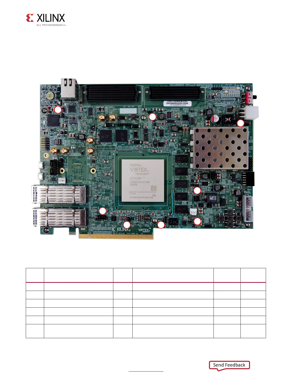
Figure 2-2 shows the VCU118 board jumper header locations. Each numbered component
shown in the figure is keyed to Table 2-3, which identifies the default jumper settings and
references the respective schematic page numbers.
X-Ref Target - Figure 2-2
Figure 2-2: VCU118 Board Header Jumper Locations
Table 2-3: Default Jumper Settings
Jumper Function Default Comments
Figure 2-2
Callout
Schematic
Page
J5 Power on reset (POR) override 2-3 U1 POR_OVERRIDE pin AG12 to GND 1 3
J7 PCIe lane size select 7-8 16-lane configuration 2 43
J8 SYSCLK source select Off SI5335A 300 MHz default 3 44
J9 USER/MGT_SI570 source select Off SI570 U32 156.250 MHz 4 45
J12 Maxim regulator inhibit Off Used when programming PWR. SYS. 5 59
J14 U30 VADJ_1V8 enable Off
Input to U25 AND, VADJ_1V8
enabled
663