VCU118 Board User Guide 22
UG1224 (v1.0) December 15, 2016
www.xilinx.com
Chapter 3: Board Component Descriptions
DDR4 Component Memory
[Figure 2-1, callout 4]
The 2.5 GB DDR4 component memory system is comprised of two sets of five 256 Mb x 16
(80-bit wide) DDR4 SDRAM devices (Micron MT40A256M16GE-075E) located at U60-U64
(C1) and U135-U139 (C2). This dual memory system is connected in 80-bit wide interfaces
to the U1 XCVU9P HP banks 71, 72, 73 (C1) and 40, 41, 42 (C2). The DDR4 0.6V VTT
termination voltages (nets DDR4_C1_VTT and DDR4_C2_VTT) are sourced from the TI
TPS51200DR linear regulators U24 and U134. The DDR4 memory interface bank VREF pins
are not connected, which, coupled with an XDC set_property INTERNAL_VREF constraint,
invoke the INTERNAL VREF mode. The connections between the C1 80-bit interface DDR4
component memories and XCVU9P banks 71, 72, and 73 are listed in Table 3-2.
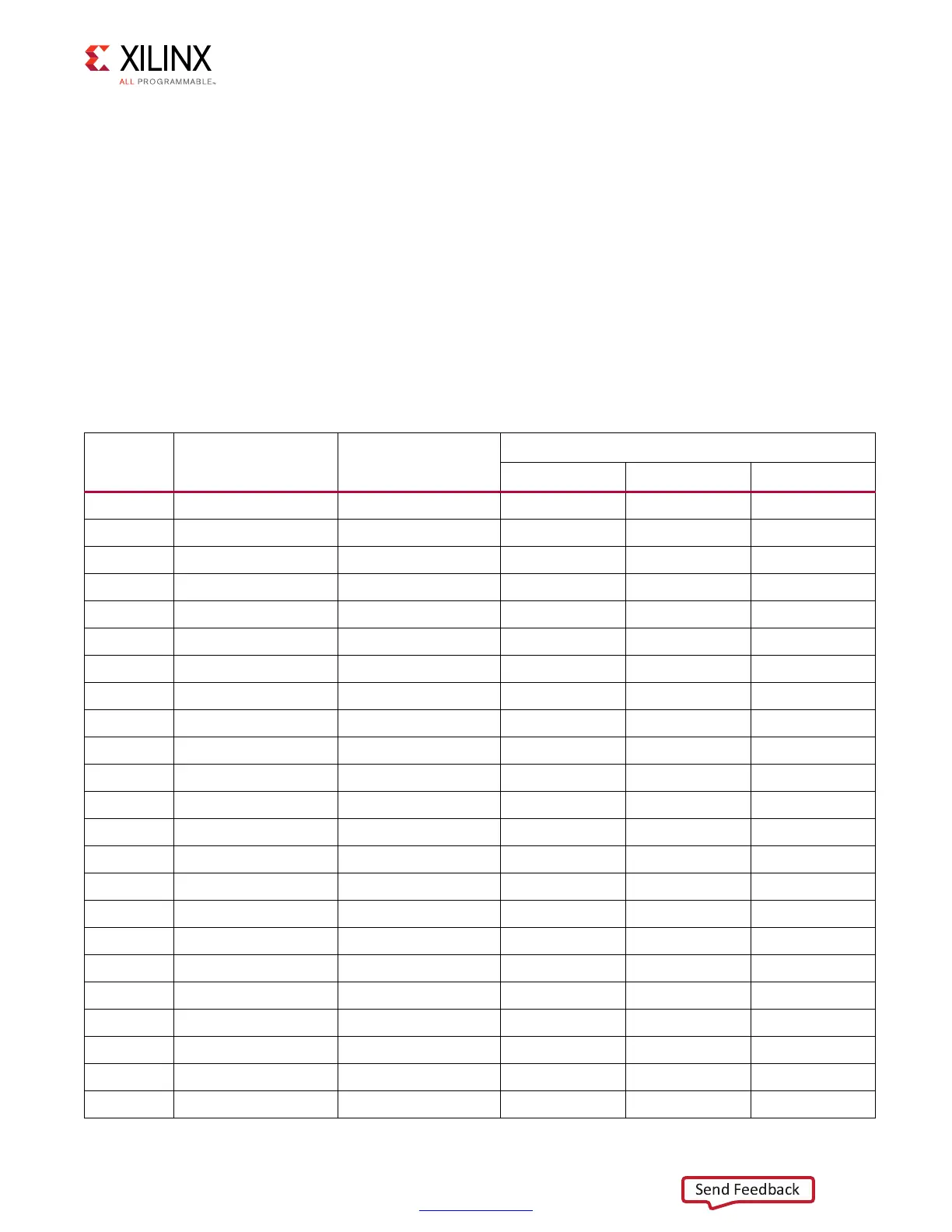
Table 3-2: DDR4 Memory 80-bit I/F C1 to FPGA U1 Banks 71, 72, and 73
FPGA (U1)
Pin
Schematic Net Name I/O Standard
Component Memory
Pin # Pin Name Ref. Des.
F11 DDR4_C1_DQ0 POD12_DCI G2 DQL0 U60
E11 DDR4_C1_DQ1 POD12_DCI F7 DQL1 U60
F10 DDR4_C1_DQ2 POD12_DCI H3 DQL2 U60
F9 DDR4_C1_DQ3 POD12_DCI H7 DQL3 U60
H12 DDR4_C1_DQ4 POD12_DCI H2 DQL4 U60
G12 DDR4_C1_DQ5 POD12_DCI H8 DQL5 U60
E9 DDR4_C1_DQ6 POD12_DCI J3 DQL6 U60
D9 DDR4_C1_DQ7 POD12_DCI J7 DQL7 U60
R19 DDR4_C1_DQ8 POD12_DCI A3 DQU0 U60
P19 DDR4_C1_DQ9 POD12_DCI B8 DQU1 U60
M18 DDR4_C1_DQ10 POD12_DCI C3 DQU2 U60
M17 DDR4_C1_DQ11 POD12_DCI C7 DQU3 U60
N19 DDR4_C1_DQ12 POD12_DCI C2 DQU4 U60
N18 DDR4_C1_DQ13 POD12_DCI C8 DQU5 U60
N17 DDR4_C1_DQ14 POD12_DCI D3 DQU6 U60
M16 DDR4_C1_DQ15 POD12_DCI D7 DQU7 U60
D11 DDR4_C1_DQS0_T DIFF_POD12_DCI G3 DQSL_T U60
D10 DDR4_C1_DQS0_C DIFF_POD12_DCI F3 DQSL_C U60
P17 DDR4_C1_DQS1_T DIFF_POD12_DCI B7 DQSU_T U60
P16 DDR4_C1_DQS1_C DIFF_POD12_DCI A7 DQSU_C U60
G11 DDR4_C1_DM0 POD12_DCI E7 DML_B/DBIL_B U60
R18 DDR4_C1_DM1 POD12_DCI E2 DMU_B/DBIU_B U60
L16 DDR4_C1_DQ16 POD12_DCI G2 DQL0 U61