VCU118 Board User Guide 47
UG1224 (v1.0) December 15, 2016
www.xilinx.com
Chapter 3: Board Component Descriptions
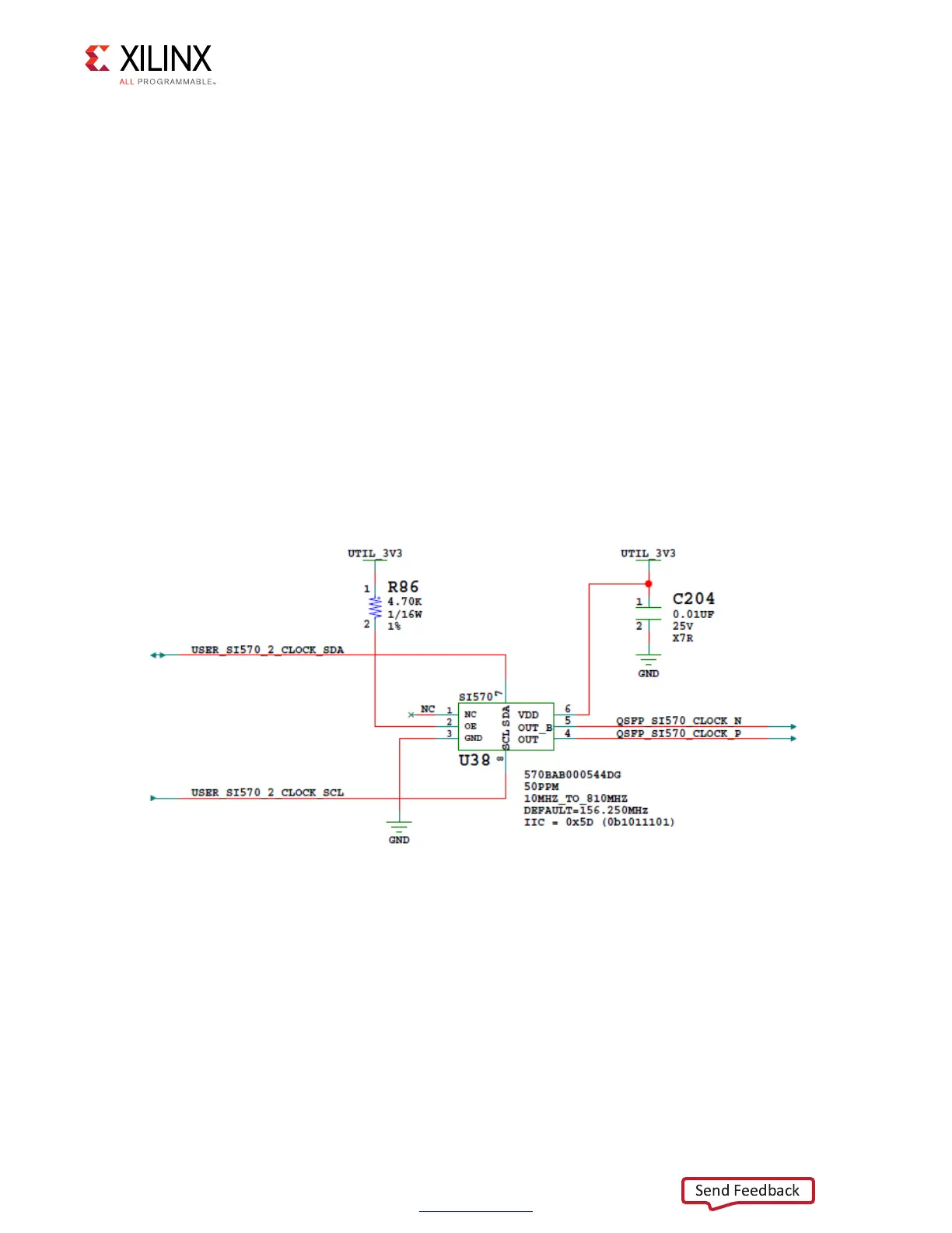
Programmable User Clock 2 (QSFP Clock)
[Figure 2-1, callout 13]
The VCU118 evaluation board has a SI570 I²C programmable low-jitter 3.3V LVDS
differential oscillator (U38) connected to FPGA U1 GTY bank 231 MGTREFCLK0 P/N pins U9
and U8 (series capacitor coupled), respectively.
On power-up, the U32 SI570 user clock defaults to an output frequency of 156.250 MHz.
The Zynq-7000 AP SoC system controller or FPGA user IP can change the output frequency
within the range of 10 MHz to 810 MHz through an I²C interface. Power cycling the VCU118
evaluation board resets the user clock to the default frequency of 156.250 MHz.
• Programmable oscillator: Silicon Labs Si570BAB0000544DG (10 MHz-810 MHz)
• Frequency tolerance: 50 ppm
• 3.3V LVDS differential output
The programmable clock circuit is shown in Figure 3-6.
X-Ref Target - Figure 3-6
Figure 3-6: VCU118 Board Programmable QSFP Clock