VCU118 Board User Guide 49
UG1224 (v1.0) December 15, 2016
www.xilinx.com
Chapter 3: Board Component Descriptions
User SMA Clock
[Figure 2-1, callout 15]
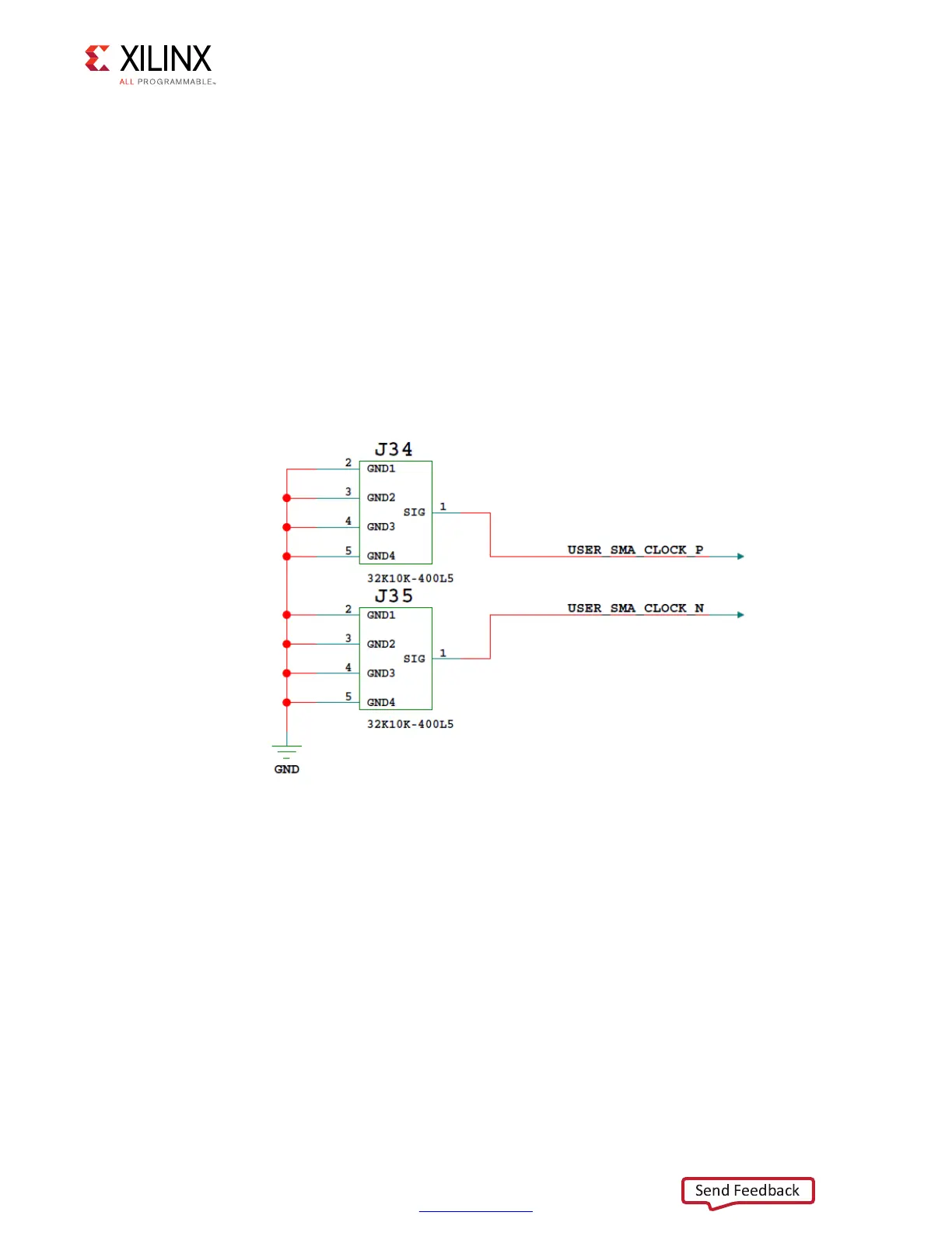
The VCU118 board provides a pair of SMAs for differential user clock input into FPGA U1 HP
bank 45. The P-side SMA J34 signal USER_SMA_CLOCK_P is connected to FPGA U1 HP bank
45 GC pin R32, with the N-side SMA J35 signal USER_SMA_CLOCK_N connected to U1 HP
bank 45 GC pin P32. Bank 45 VADJ_1V8_FPGA VCCO is nominally 1.8V. The
USER_SMA_CLOCK input voltage swing should not exceed the voltage setting on the
VADJ_1V8_FPGA rail. Any signal connected to the USER_SMA_CLOCK connector inputs must
be equal to or less than the VCCO for bank 45. Valid values for the VADJ rail VADJ_1V8_FPGA
are 1.5V and 1.8V. This value must be confirmed prior to applying signals to the
USER_SMA_CLOCK connectors.
X-Ref Target - Figure 3-8
Figure 3-8: User SMA Clock