VCU118 Board User Guide 68
UG1224 (v1.0) December 15, 2016
www.xilinx.com
Chapter 3: Board Component Descriptions
PCI Express Endpoint Connectivity
[Figure 2-1, callout 17]
The 16-lane PCI Express edge connector U2 performs data transfers at the rate of 2.5 GT/s
for Gen1 applications, 5.0 GT/s for Gen2 applications, and 8.0 GT/s for Gen3 applications.
The PCIe transmit and receive signal data paths have a characteristic impedance of
85Ω ±10%. The PCIe clock is routed as a 100Ω differential pair.
The XCVU9P-L2FLGA2104 (-2 speed grade) is deployed on the VCU118 to support up to
Gen3 x8.
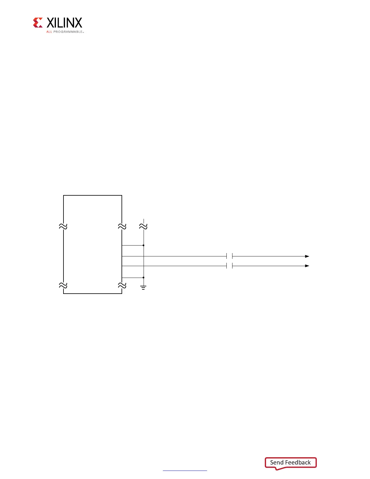
The PCIe reference clock input is from the U2 edge connector. It is AC coupled to FPGA U1
through the MGTREFCLK0 pins of Quad 225. PCIE_CLK_Q0_P is connected to U1 pin AL9,
and the _N net is connected to pin AL8. The PCI Express clock connection is shown in
Figure 3-10.
The PCIe clock is routed to a 1-to-2 ICS85411A clock buffer U20. The Q0 output of U20 is
wired to the GTY225 MGTHREFCLK0 input (see Table 3-15). The Q1 output of U20 is wired to
the GTY227 MGTHREFCLK0 input (see Table 3-17). The 1-to-2 U20 PCIe clock buffer circuit
is shown in Figure 3-11.
X-Ref Target - Figure 3-10
Figure 3-10: PCIe Edge Connector Clock
PCI Express
Eight-Lane
Edge Connector
OE
GND
REFCLK+
REFCLK-
GND
A12
A13
A14
A15
PCIE_CLK_Q0_C_P
PCIE_CLK_Q0_C_N
GND
PCIE_CLK_Q0_P
PCIE_CLK_Q0_N
C62
0.22 μf
0.22 μf
C63
U2
X18024-100616