VCU118 Board User Guide 74
UG1224 (v1.0) December 15, 2016
www.xilinx.com
Chapter 3: Board Component Descriptions
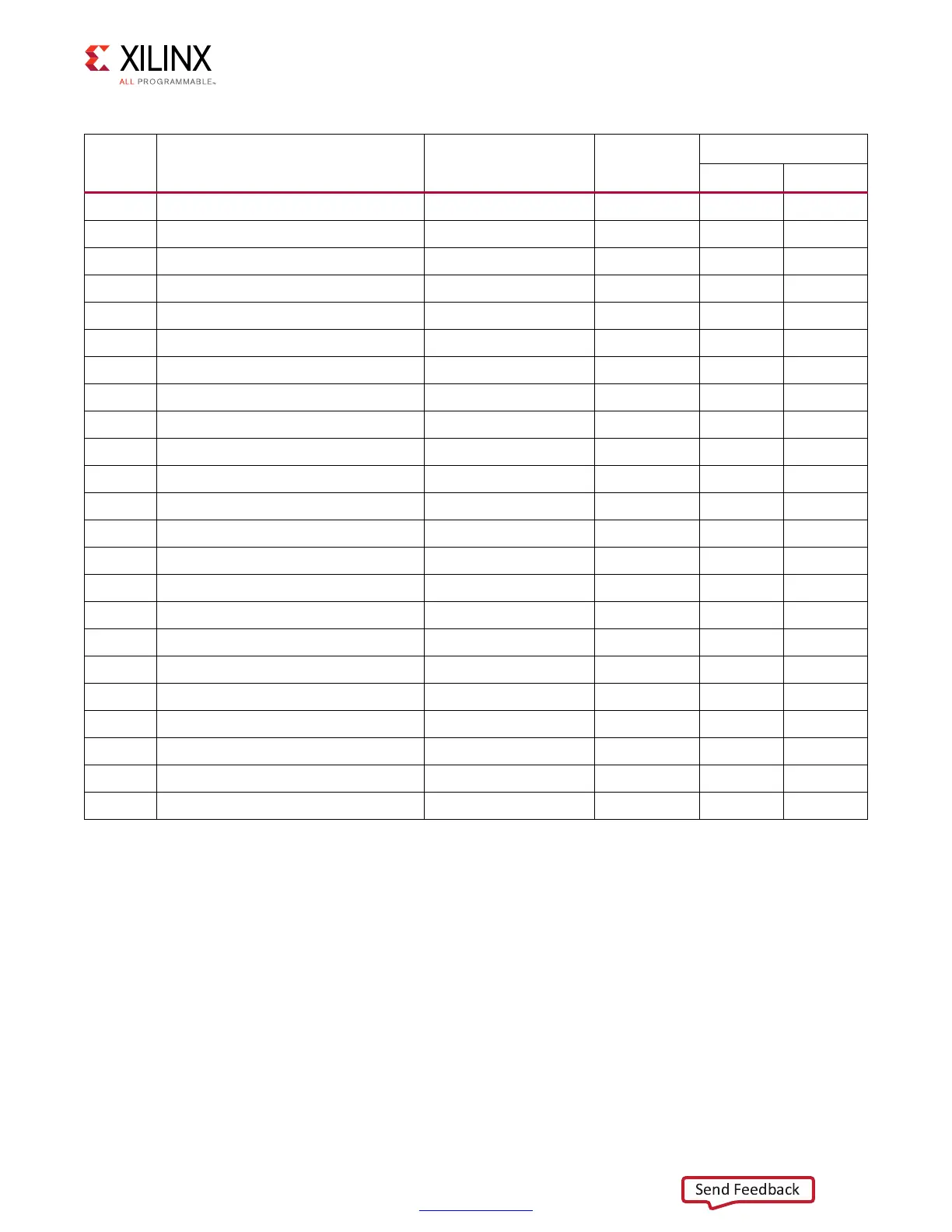
Table 3-23: VCU118 Board FPGA U1 to QSFP+ Module QSFP2 U123 Connections
FPGA
(U1) Pin
FPGA (U1) Pin Name Schematic Net Name
FPGA (U1)
Direction
QSFP2 U123
Pin Num Pin Name
L5 MGTYTXP0_232 QSFP2_TX1_P Output 36 TX1P
L4 MGTYTXN0_232 QSFP2_TX1_N Output 37 TX1N
T2 MGTYRXP0_232 QSFP2_RX1_P Input 17 RX1P
T1 MGTYRXN0_232 QSFP2_RX1_N Input 18 RX1N
K7 MGTYTXP1_232 QSFP2_TX2_P Output 3 TX2P
K6 MGTYTXN1_232 QSFP2_TX2_N Output 2 TX2N
R4 MGTYRXP1_232 QSFP2_RX2_P Input 22 RX2P
R3 MGTYRXN1_232 QSFP2_RX2_N Input 21 RX2N
J5 MGTYTXP2_232 QSFP2_TX3_P Output 33 TX3P
J4 MGTYTXN2_232 QSFP2_TX3_N Output 34 TX3N
P2 MGTYRXP2_232 QSFP2_RX3_P Input 14 RX3P
P1 MGTYRXN2_232 QSFP2_RX3_N Input 15 RX3N
H7 MGTYTXP3_232 QSFP2_TX4_P Output 6 TX4P
H6 MGTYTXN3_232 QSFP2_TX4_N Output 5 TX4N
M2 MGTYRXP3_232 QSFP2_RX4_P Input 25 RX4P
M1 MGTYRXN3_232 QSFP2_RX4_N Input 24 RX4N
U28.11 SC3 QSFP2_IIC_SCL(1) Output 11 SCL
U28.10 SD3 QSFP2_IIC_SDA(1) BiDir 12 SDA
AN23 IO_L20N_T3L_N3_AD1N_64 QSFP2_MODSELL(2) Output 8 MODSELL
AY22 IO_L10P_T1U_N6_QBC_AD4P_64 QSFP2_RESETL(2) Output 9 RESETL
AN24 IO_L20P_T3L_N2_AD1P_64 QSFP2_MODPRSL(2) Output 27 MODPRSL
AT21 IO_T2U_N12_64 QSFP2_INTL(2) Input 28 INTL
AT24 IO_L18N_T2U_N11_AD2N_64 QSFP2_LPMODE(2) Output 31 LPMODE
Notes:
1. The QSFP+ connector U123 I
2
C SCL/SDA IS connected to the I
2
C switch U28 to the IIC_MAIN_SCL/SDA bus. See I2C Bus,
Topology, and Switches.
2. The QSFP+ connector U123 QSFP2 control signals are level-shifted by U3.
For additional information about the quad small form factor pluggable (28 Gb/s QSFP+) module, see the SFF-8663
specification for the 28 Gb/s QSFP+ at the SFF-8663 specification website [Ref 24].