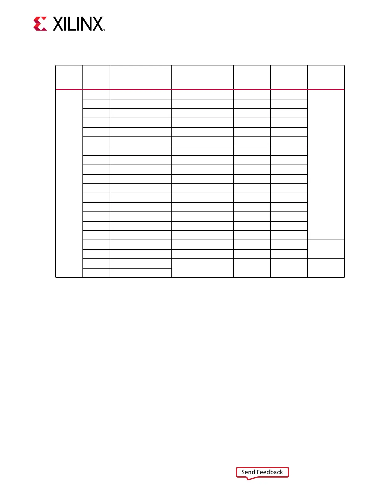
Table 12: XCVU37P U1 GTY Transceiver Bank 135 Connections
MGT
Bank
FPGA
(U1)
Pin
FPGA (U1) Pin
Name
Schematic Net
Name
Connected
Pin
Connected
Pin Name
Connected
Device
GTY bank
135
G48 MGTYTXP0_135 QSFP1_TX1_P 36 TX1P
QSFP1 J42
G49
MGTYTXN0_135 QSFP1_TX1_N 37 TX1N
G53 MGTYRXP0_135 QSFP1_RX1_P 17 RX1P
G54 MGTYRXN0_135 QSFP1_RX1_N 18 RX1N
E48 MGTYTXP1_135 QSFP1_TX2_P 3 TX2P
E49 MGTYTXN1_135 QSFP1_TX2_N 2 TX2N
F51 MGTYRXP1_135 QSFP1_RX2_P 22 RX2P
F52 MGTYRXN1_135 QSFP1_RX2_N 21 RX2N
C48 MGTYTXP2_135 QSFP1_TX3_P 33 TX3P
C49 MGTYTXN2_135 QSFP1_TX3_N 34 TX3N
E53 MGTYRXP2_135 QSFP1_RX3_P 14 RX3P
E54 MGTYRXN2_135 QSFP1_RX3_N 15 RX3N
A49 MGTYTXP3_135 QSFP1_TX4_P 6 TX4P
A50 MGTYTXN3_135 QSFP1_TX4_N 5 TX4N
D51 MGTYRXP3_135 QSFP1_RX4_P 25 RX4P
D52 MGTYRXN3_135 QSFP1_RX4_N 24 RX4N
P42 MGTREFCLK0P_135 QSFP_SI570_CLOCK_P
1
4 OUT
U95 SI570 I2C
prog. osc.
P43 MGTREFCLK0N_135 QSFP_SI570_CLOCK_N
1
5 OUT_B
M42 MGTREFCLK1P_135
NC NC NC NC
M43 MGTREFCLK1N_135
Notes:
1. Series 0.01 μF capacitor coupled.
Chapter 3: Board Component Descriptions
UG1302 (v1.0) December 21, 2018 www.xilinx.com
VCU128 Board User Guide 53