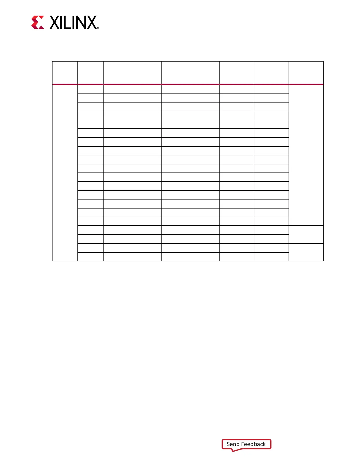
Table 14: XCVU37P U1 GTY Transceiver Bank 132 Connections
MGT
Bank
FPGA
(U1)
Pin
FPGA (U1) Pin
Name
Schematic Net
Name
Connected
Pin
Connected
Pin Name
Connected
Device
GTY bank
132
V46 MGTYTXP0_132 QSFP3_TX1_P 36 TX1P
QSFP2 J35
V47
MGTYTXN0_132 QSFP3_TX1_N 37 TX1N
U53 MGTYRXP0_132 QSFP3_RX1_P 17 RX1P
U54 MGTYRXN0_132 QSFP3_RX1_N 18 RX1N
U44 MGTYTXP1_132 QSFP3_TX2_P 3 TX2P
U45 MGTYTXN1_132 QSFP3_TX2_N 2 TX2N
U49 MGTYRXP1_132 QSFP3_RX2_P 22 RX2P
U50 MGTYRXN1_132 QSFP3_RX2_N 21 RX2N
T46 MGTYTXP2_132 QSFP3_TX3_P 33 TX3P
T47 MGTYTXN2_132 QSFP3_TX3_N 34 TX3N
T51 MGTYRXP2_132 QSFP3_RX3_P 14 RX3P
T52 MGTYRXN2_132 QSFP3_RX3_N 15 RX3N
R44 MGTYTXP3_132 QSFP3_TX4_P 6 TX4P
R45 MGTYTXN3_132 QSFP3_TX4_N 5 TX4N
R53 MGTYRXP3_132 QSFP3_RX4_P 25 RX4P
R54 MGTYRXN3_132 QSFP3_RX4_N 24 RX4N
Y42 MGTREFCLK0P_132 QSFP3_SI570_CLOCK_P
1
4 OUT
U82 SI570 I2C
prog. osc.
Y43 MGTREFCLK0N_132 QSFP3_SI570_CLOCK_N
1
5 OUT_B
W40 MGTREFCLK1P_132 SI5328_CLOCK2_C_P
1
35 CKOUT2_P
U87 SI5328B
jitter atten.
W41 MGTREFCLK1N_132 SI5328_CLOCK2_C_N
1
34 CKOUT2_N
Notes:
1. Series 0.01uF capacitor coupled.
Chapter 3: Board Component Descriptions
UG1302 (v1.0) December 21, 2018 www.xilinx.com
VCU128 Board User Guide 55