EasyManuals Logo

Xilinx Virtex-5 FPGA ML561 User Manual

Xilinx Virtex-5 FPGA ML561
140 pages
To Next Page IconTo Next Page
To Previous Page IconTo Previous Page
Page #60 background imageLoading...
Page #60 background image
60 www.xilinx.com Virtex-5 FPGA ML561 User Guide
UG199 (v1.2.1) June 15, 2009
Chapter 7: ML561 Hardware-Simulation Correlation
R
DDR2 DQ is a bidirectional signal. To perform hardware measurements for a Write
operation that is not interrupted by a Read response or a Refresh operation, the testbench
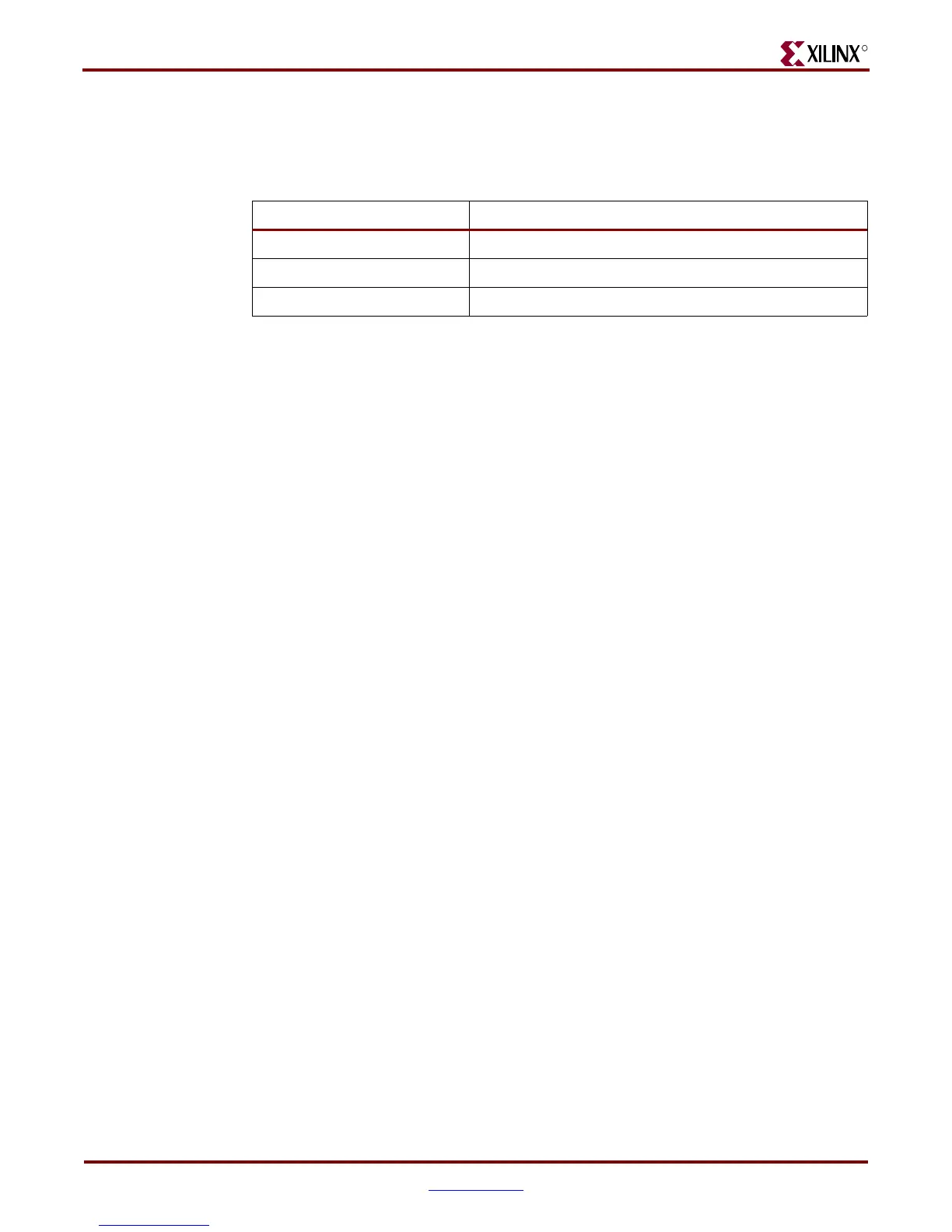
on FPGA1 is controlled by DIP switches (SW2) as indicated in Table 7-3.
Table 7-3: DIP[1:2] Settings
Setting Description
2’b00 or 2’b11 Normal alternating Write/Read sequence
2’b01 Write only, Refresh disabled
2’b10 Write once, then Read only, Refresh disabled

Table of Contents

Questions and Answers:

Question and Answer IconNeed help?

Do you have a question about the Xilinx Virtex-5 FPGA ML561 and is the answer not in the manual?

Xilinx Virtex-5 FPGA ML561 Specifications

General IconGeneral
BrandXilinx
ModelVirtex-5 FPGA ML561
CategoryMotherboard
LanguageEnglish

Related product manuals