ZCU102 Evaluation Board User Guide www.xilinx.com 102
UG1182 (v1.2) March 20, 2017
Chapter 3: Board Component Descriptions
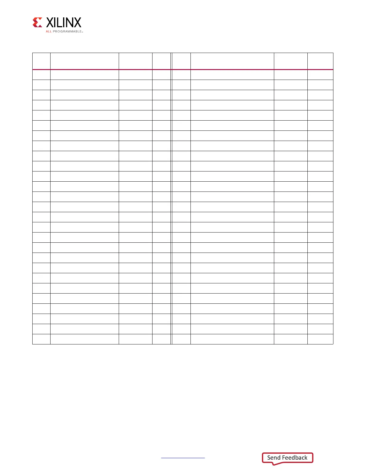
Table 3-52: J4 HPC1 FMC Section G and H Connections to XCZU9EG U1
J5 Pin Schematic Net Name
I/O
Standard
U1 Pin J5 Pin Schematic Net Name
I/O
Standard
U1 Pin
G2 FMC_HPC1_CLK1_M2C_P LVDS P10 H1 NC
G3 FMC_HPC1_CLK1_M2C_N LVDS P9 H2 FMC_HPC1_PRSNT_M2C_B
(1)
G6 FMC_HPC1_LA00_CC_P LVDS AE5 H4 FMC_HPC1_CLK0_M2C_P LVDS AE7
G7 FMC_HPC1_LA00_CC_N LVDS AF5 H5 FMC_HPC1_CLK0_M2C_N LVDS AF7
G9 FMC_HPC1_LA03_P
LVCMOS18 AH1 H7 FMC_HPC1_LA02_P LVCMOS18 AD2
G10 FMC_HPC1_LA03_N
LVCMOS18 AJ1 H8 FMC_HPC1_LA02_N LVCMOS18 AD1
G12 FMC_HPC1_LA08_P
LVCMOS18 AE3 H10 FMC_HPC1_LA04_P LVCMOS18 AF2
G13 FMC_HPC1_LA08_N
LVCMOS18 AF3 H11 FMC_HPC1_LA04_N LVCMOS18 AF1
G15 FMC_HPC1_LA12_P
LVCMOS18 AD7 H13 FMC_HPC1_LA07_P LVCMOS18 AD4
G16 FMC_HPC1_LA12_N
LVCMOS18 AD6 H14 FMC_HPC1_LA07_N LVCMOS18 AE4
G18 FMC_HPC1_LA16_P
LVCMOS18 AG10 H16 FMC_HPC1_LA11_P LVCMOS18 AE8
G19 FMC_HPC1_LA16_N
LVCMOS18 AG9 H17 FMC_HPC1_LA11_N LVCMOS18 AF8
G21 FMC_HPC1_LA20_P
LVCMOS18 AB11 H19 FMC_HPC1_LA15_P LVCMOS18 AD10
G22 FMC_HPC1_LA20_N
LVCMOS18 AB10 H20 FMC_HPC1_LA15_N LVCMOS18 AE9
G24 FMC_HPC1_LA22_P
LVCMOS18 AF11 H22 FMC_HPC1_LA19_P LVCMOS18 AA11
G25 FMC_HPC1_LA22_N
LVCMOS18 AG11 H23 FMC_HPC1_LA19_N LVCMOS18 AA10
G27 FMC_HPC1_LA25_P
LVCMOS18 AE10 H25 FMC_HPC1_LA21_P LVCMOS18 AC12
G28 FMC_HPC1_LA25_N
LVCMOS18 AF10 H26 FMC_HPC1_LA21_N LVCMOS18 AC11
G30 FMC_HPC1_LA29_P
LVCMOS18 W12 H28 FMC_HPC1_LA24_P LVCMOS18 AH12
G31 FMC_HPC1_LA29_N
LVCMOS18 W11 H29 FMC_HPC1_LA24_N LVCMOS18 AH11
G33 FMC_HPC1_LA31_P NC H31 FMC_HPC1_LA28_P
LVCMOS18 T13
G34 FMC_HPC1_LA31_N NC H32 FMC_HPC1_LA28_N
LVCMOS18 R13
G36 FMC_HPC1_LA33_P NC H34 FMC_HPC1_LA30_P NC
G37 FMC_HPC1_LA33_N NC H35 FMC_HPC1_LA30_N NC
G39 VADJ_FMC_BUS H37 FMC_HPC1_LA32_P NC
H38 FMC_HPC1_LA32_N NC
H40 VADJ_FMC_BUS
Notes:
1. FMC_HPC0_PRSNT_M2C_B is the HPC FMC JTAG bypass switch U27.4 OE control signal is driven from I2C I/O expander
U97.13.